SLVSE94G September 2018 – June 2024 TPS2663
PRODUCTION DATA
- 1
- 1 Features
- 2 Applications
- 3 Description
- 4 Device Comparison Table
- 5 Pin Configuration and Functions
- 6 Specifications
- 7 Parameter Measurement Information
-
8 Detailed Description
- 8.1 Overview
- 8.2 Functional Block Diagram
- 8.3
Feature Description
- 8.3.1 Hot Plug-In and Inrush Current Control
- 8.3.2 PGOOD and PGTH
- 8.3.3 Undervoltage Lockout (UVLO)
- 8.3.4 Overvoltage Protection (OVP)
- 8.3.5 Input Reverse Polarity Protection (B_GATE, DRV)
- 8.3.6 Reverse Current Protection
- 8.3.7 Overload and Short-Circuit Protection
- 8.3.8 Output Power Limiting, PLIM (TPS26632, TPS26633, TPS26635, TPS26636, and TPS26637 Only)
- 8.3.9 Current Monitoring Output (IMON)
- 8.3.10 FAULT Response (FLT)
- 8.3.11 IN_SYS, IN, OUT, and GND Pins
- 8.3.12 Thermal Shutdown
- 8.3.13 Low Current Shutdown Control (SHDN)
- 8.4 Device Functional Modes
-
9 Application and Implementation
- 9.1 Application Information
- 9.2
Typical Application: Power Path Protection in a PLC System
- 9.2.1 Design Requirements
- 9.2.2 Detailed Design Procedure
- 9.2.3 Application Curves
- 9.3 System Examples
- 9.4 Dos and Do Nots
- 9.5 Power Supply Recommendations
- 9.6 Layout
- 10Device and Documentation Support
- 11Revision History
- 12Mechanical, Packaging, and Orderable Information
Package Options
Refer to the PDF data sheet for device specific package drawings
Mechanical Data (Package|Pins)
- RGE|24
- PWP|20
Thermal pad, mechanical data (Package|Pins)
Orderable Information
9.3.2 Priority Power MUX Operation
Applications having two energy sources, such as portable battery powered equipment require preference of one source to another. For example, mains power (wall-adapter) has the priority over the internal backup power or auxiliary power. These applications demand for switch over from mains power to backup power only when main input voltage falls below a user defined threshold. The TPS2663x devices provide a simple solution for priority power multiplexing needs.
Figure 9-12 shows a typical priority power multiplexing implementation using devices. When the MAIN power is present, the device in VIN_MAIN path powers the OUT bus irrespective of whether auxiliary power VIN_AUX is greater than or less than VIN_MAIN. After the voltage on the VIN_MAIN rail falls below the user-defined threshold, the device VIN_MAIN issues a signal to switch over to auxiliary power VIN_AUX. The transition happens seamlessly in tOVP(dly_fast), with minimal voltage droop on the output. The voltage droop during transition is a function of load current and output capacitance. See Equation 13.

where
- V(DROOP) is in volts, I(LOAD) is load current in Ampere, C(OUT) is output capacitance in µF, tOVP(fast_dly) = 140 µs (typical)
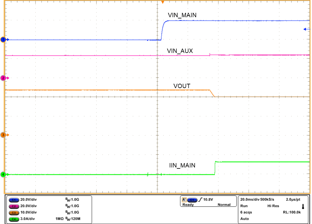
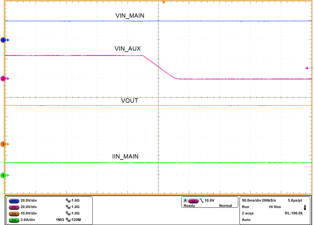
Figure 9-13, Figure 9-14, Figure 9-15 and figure 9-16 show typical switch-over waveforms of Priority Muxing implementation using the TPS26630 or TPS26631 for 20-V primary and 24-V auxiliary bus.
 Figure 9-12 Priority Power Mux Implementation


