SLVSE42B October   2017  – September 2019 TPS27S100

PRODUCTION DATA.  

  1. Features
  2. Applications
  3. Description
    1.     Typical Application Schematic
  4. Revision History
  5. Pin Configuration and Functions
    1.     Pin Functions
  6. Specifications
    1. 6.1 Absolute Maximum Ratings
    2. 6.2 ESD Ratings
    3. 6.3 Recommended Operating Conditions
    4. 6.4 Thermal Information
    5. 6.5 Electrical Characteristics
    6. 6.6 Timing Requirements – Current Monitor Characteristics
    7. 6.7 Switching Characteristics
    8. 6.8 Typical Characteristics
  7. Detailed Description
    1. 7.1 Overview
    2. 7.2 Functional Block Diagram
    3. 7.3 Feature Description
      1. 7.3.1 Accurate Current Monitor
      2. 7.3.2 Adjustable Current Limit
      3. 7.3.3 Inductive-Load Switching-Off Clamp
      4. 7.3.4 Full Protections and Diagnostics
        1. 7.3.4.1 Short-to-GND and Overload Detection
        2. 7.3.4.2 Open-Load Detection
        3. 7.3.4.3 Short-to-Supply Detection
        4. 7.3.4.4 Thermal Fault Detection
        5. 7.3.4.5 UVLO Protection
        6. 7.3.4.6 Loss of GND Protection
        7. 7.3.4.7 Reverse Current Protection
        8. 7.3.4.8 Protection for MCU I/Os
    4. 7.4 Device Functional Modes
      1. 7.4.1 Working Mode
  8. Application and Implementation
    1. 8.1 Application Information
    2. 8.2 Typical Application
      1. 8.2.1 Design Requirements
      2. 8.2.2 Detailed Design Procedure
      3. 8.2.3 Application Curves
  9. Power Supply Recommendations
  10. 10Layout
    1. 10.1 Layout Guidelines
    2. 10.2 Layout Example
      1. 10.2.1 Without a GND Network
      2. 10.2.2 With a GND Network
  11. 11Device and Documentation Support
    1. 11.1 Receiving Notification of Documentation Updates
    2. 11.2 Community Resources
    3. 11.3 Trademarks
    4. 11.4 Electrostatic Discharge Caution
    5. 11.5 Glossary
  12. 12Mechanical, Packaging, and Orderable Information

Package Options

Mechanical Data (Package|Pins)
Thermal pad, mechanical data (Package|Pins)
Orderable Information

Typical Characteristics

All the below data are based on the mean value of the three lots samples, VIN = 24 V if not specified.
TPS27S100 D001_SLVSCM2.gif
Figure 5. IN Pin Undervoltage Rising and Falling Thresholds VIN,UVR and VIN,UVF
TPS27S100 D004_SLVSE42.gif
Figure 7. Ioff,diag as a Function of Temperature
TPS27S100 D006_SLVSE42.gif
Figure 9. Drain-to-source Diode Voltage VF
TPS27S100 D008_SLVSE42.gif
Figure 11. FET RDSON
TPS27S100 D010_SLVSE42.gif
Figure 13. TDon and TDoff
TPS27S100 D013_SLVSE42.gif
Figure 15. Vol,off
TPS27S100 D015_SLVSE42.gif
Figure 17. K(IMON) at IOUT = 5 mA, VIN = 24 V
TPS27S100 D019_SLVSE42.gif
Figure 19. K(IMON) at IOUT = 50 mA, VIN = 24 V
TPS27S100 D018_SLVSCM2.gif
Figure 21. K(IMON) at IOUT = 1 A, VIN = 24 V
TPS27S100 D021_SLVSCM2.gif
Figure 23. K(ILIM) at IILIM = 1.6 A, VIN = 24 V
TPS27S100 D002_SLVSE42.gif
Figure 6. Inom With No Load and 24-Ω Load
TPS27S100 D005_SLVSCM2.gif
Figure 8. Vlogic,h and Vlogic,l
TPS27S100 D007_SLVSCM2.gif
Figure 10. VDS, Clamp
TPS27S100 D009_SLVSE42.gif
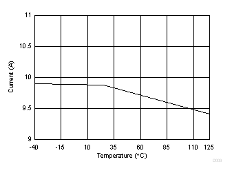
Figure 12. Current Limit Ilim,nom
TPS27S100 D011_SLVSE42.gif
Figure 14. dV/dtON and dV/dtOFF
TPS27S100 D014_SLVSCM2.gif
Figure 16. Iol,on
TPS27S100 D017_SLVSE42.gif
Figure 18. K(IMON) at IOUT = 25 mA, VIN = 24 V
TPS27S100 D016_SLVSCM2.gif
Figure 20. K(IMON) at IOUT = 100 mA, VIN = 24 V
TPS27S100 D020_SLVSE42.gif
Figure 22. K(ILIM) at IILIM = 0.5 A, VIN = 24 V