SLUS791A July 2007 – September 2015 TPS28226
PRODUCTION DATA.
- 1 Features
- 2 Applications
- 3 Description
- 4 Revision History
- 5 Pin Configuration and Functions
- 6 Specifications
- 7 Detailed Description
- 8 Application and Implementation
- 9 Power Supply Recommendations
- 10Layout
- 11Device and Documentation Support
- 12Mechanical, Packaging, and Orderable Information
Package Options
Mechanical Data (Package|Pins)
Thermal pad, mechanical data (Package|Pins)
- DRB|8
Orderable Information
7 Detailed Description
7.1 Overview
The TPS28226 features a 3-state PWM input compatible with all multi-phase controllers employing 3-state output feature. As long as the input stays within 3-state window for the 250-ns hold-off time, the driver switches both outputs low. This shutdown mode prevents a load from the reversed- output-voltage.
The other features include undervoltage lockout, thermal shutdown and two-way enable/power good signal. Systems without 3-state featured controllers can use enable/power good input/output to hold both outputs low during shutting down.
The TPS28226 is offered in an economical SOIC-8 and thermally enhanced low-size Dual Flat No-Lead (DFN-8) packages. The driver is specified in the extended temperature range of –40°C to 125°C with the absolute maximum junction temperature 150°C.
7.2 Functional Block Diagram
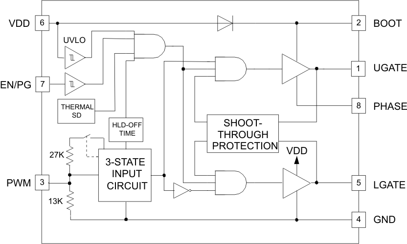
7.3 Feature Description
7.3.1 Undervoltage Lockout (UVLO)
The TPS28226 incorporates an under voltage lockout circuit that keeps the driver disabled and external power FETs in an OFF state when the input supply voltage VDD is insufficient to drive external power FETs reliably. During power up, both gate drive outputs remain low until voltage VDD reaches UVLO threshold, typically 6.35 V. Once the UVLO threshold is reached, the condition of the gate drive outputs is defined by the input PWM and EN/PG signals. During power down the UVLO threshold is set lower, typically 5.0 V. The 1.35 V for the TPS28226 hysteresis is selected to prevent the driver from turning ON and OFF while the input voltage crosses UVLO thresholds, especially with low slew rate. The TPS28226 has the ability to send a signal back to the system controller that the input supply voltage VDD is insufficient by internally pulling down the EN/PG pin. The TPS28226 releases EN/PG pin immediately after the VDD has risen above the UVLO threshold.
7.3.2 Output Active Low
The output active-low circuit effectively keeps the gate outputs low even if the driver is not powered up. This prevents open-gate conditions on the external power FETs and accidental turn on when the main power-stage supply voltage is applied before the driver is powered up. For the simplicity, the output active low circuit is shown in a block diagram as the resistor connected between LGATE and GND pins with another one connected between UGATE and PHASE pins.
7.3.3 Enable/Power Good
The Enable/Power Good circuit allows the TPS28226 to follow the PWM input signal when the voltage at EN/PG pin is above 2.1 V maximum. This circuit has a unique two-way communication capability. This is illustrated by Figure 20.
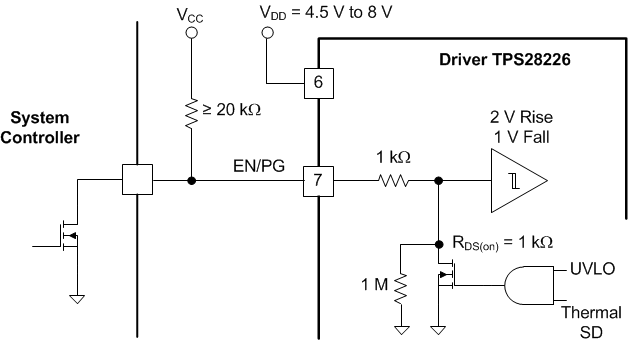 Figure 20. Enable/Power Good Circuit
The EN/PG pin has approximately 1-kΩ internal series resistor. Pulling EN/PG high by an external ≥ 20-kΩ resistor allows two-way communication between controller and driver. If the input voltage VDD is below UVLO threshold or thermal shut down occurs, the internal MOSFET pulls EN/PG pin to GND through 1-kΩ resistor. The voltage across the EN/PG pin is now defined by the resistor divider comprised by the external pull up resistor, 1-kΩ internal resistor and the internal FET having 1-kΩ RDS(on). Even if the system controller allows the driver to start by setting its own enable output transistor OFF, the driver keeps the voltage at EN/PG low. Low EN/PG signal indicates that the driver is not ready yet because the supply voltage VDD is low or that the driver is in thermal shutdown mode. The system controller can arrange the delay of PWM input signals coming to the driver until the driver releases EN/PG pin. If the input voltage VDD is back to normal, or the driver is cooled down below its lower thermal shutdown threshold, then the internal MOSFET releases the EN/PG pin and normal operation resumes under the external Enable signal applied to EN/PG input. Another feature includes an internal 1-MΩ resistor that pulls EN/PG pin low and disables the driver in case the system controller accidentally loses connection with the driver. This could happen if, for example, the system controller is located on a separate PCB daughter board.
The EN/PG pin can serve as the second pulse input of the driver additionally to PWM input. The delay between EN/PG and the UGATE going high, provided that PWM input is also high, is only about 30 ns. If the PWM input pulses are synchronized with EN/PG input, then when PWM and EN/PG are high, the UGATE is high and LGATE is low. If both PWM and EN/PG are low, then UGATE and LGATE are both low as well. This means the driver allows operation of a synchronous buck regulator as a conventional buck regulator using the body diode of the low-side power MOSFET as the freewheeling diode. This feature can be useful in some specific applications to allow startup with a pre-biased output or, to improve the efficiency of buck regulator when in power saving mode with low output current.
7.3.4 3-State Input
As soon as the EN/PG pin is set high and input PWM pulses are initiated (see Note below). The dead-time control circuit ensures that there is no overlapping between UGATE and LGATE drive outputs to eliminate shoot through current through the external power FETs. Additionally to operate under periodical pulse sequencing, the TPS28226 has a self-adjustable PWM 3-state input circuit. The 3-state circuit sets both gate drive outputs low, and thus turns the external power FETs OFF if the input signal is in a high impedance state for at least 250 ns typical. At this condition, the PWM input voltage level is defined by the internal 27-kΩ to 13-kΩ resistor divider shown in the block diagram. This resistor divider forces the input voltage to move into the 3-state window. Initially the 3-state window is set between 1.0-V and 2.0-V thresholds. The lower threshold of the 3-state window is always fixed at about 1.0 V. The higher threshold is adjusted to about 75% of the input signal amplitude. The self-adjustable upper threshold allows shorter delay if the input signal enters the 3-state window while the input signal was high, thus keeping the high-side power FET in ON state just slightly longer than 250 ns time constant set by an internal 3-state timer. Both modes of operation, PWM input pulse sequencing and the 3-state condition, are illustrated in the timing diagrams shown in Figure 19. The self-adjustable upper threshold allows operation in wide range amplitude of input PWM pulse signals. After entering into the 3-state window and staying within the window for the hold-off time, the PWM input signal level is defined by the internal resistor divider and, depending on the input pulse amplitude, can be pulled up above the normal PWM pulse amplitude (Figure 21) or down below the normal input PWM pulse (Figure 22).
7.3.4.1 TPS28226 3-State Exit Mode
- To exit the 3-state operation mode, the PWM signal should go high and then low at least once.
This is necessary to restore the voltage across the bootstrap capacitor that could be discharged during the 3-state mode if the 3-state condition lasts long enough.
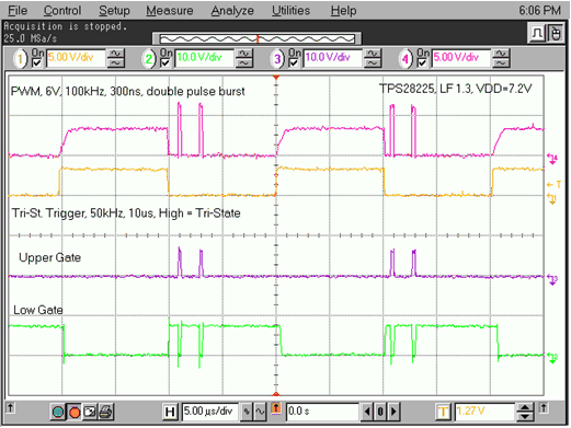 Figure 21. 6-V Amplitude PWM Pulse (TPS28225 example)
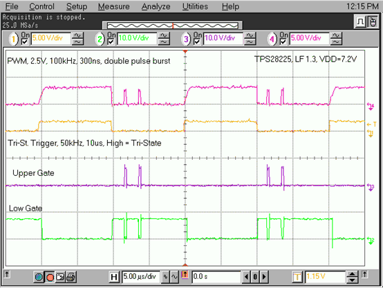 Figure 22. 2.5-V Amplitude PWM Pulse (TPS28225 example)
NOTE
The driver sets UGATE low and LGATE high when PWM is low. When the PWM goes high, UGATE goes high and LGATE goes low.
7.3.4.2 External Resistor Interference
Any external resistor between PWM input and GND with the value lower than 40 kΩ can interfere with the 3-state thresholds. If the driver is intended to operate in the 3-state mode, any resistor below 40 kΩ at the PWM and GND should be avoided. A resistor lower than 3.5 kΩ connected between the PWM and GND completely disables the 3-state function. In such case, the 3-state window shrinks to zero and the lower 3-state threshold becomes the boundary between the UGATE staying low and LGATE being high and vice versa depending on the PWM input signal applied. It is not necessary to use a resistor <3.5 kΩ to avoid the 3-state condition while using a controller that is 3-state capable. If the rise and fall time of the input PWM signal is shorter than 250 ns, then the driver never enters into the 3-state mode.
In the case where the low-side MOSFET of a buck converter stays on during shutdown, the 3-state feature can be fused to avoid negative resonant voltage across the output capacitor. This feature also can be used during start up with a pre-biased output in the case where pulling the output low during the startup is not allowed due to system requirements. If the system controller does not have the 3-state feature and never goes into the high-impedance state, then setting the EN/PG signal low will keep both gate drive outputs low and turn both low- and high-side MOSFETs OFF during the shut down and start up with the pre-biased output.
The self-adjustable input circuit accepts wide range of input pulse amplitudes (2 V up to 13.2 V) allowing use of a variety of controllers with different outputs including logic level. The wide PWM input voltage allows some flexibility if the driver is used in secondary side synchronous rectifier circuit. The operation of the TPS28226 with a 12-V input PWM pulse amplitude, and with VDD = 7.2 V and VDD = 5 V respectively is shown in Figure 23 and Figure 24.
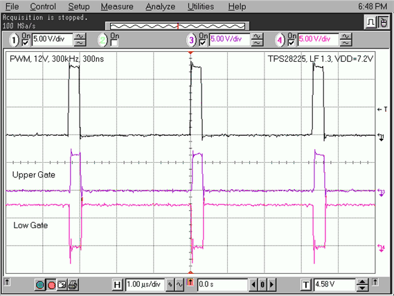 Figure 23. 12-V PWM Pulse at VDD = 7.2 V
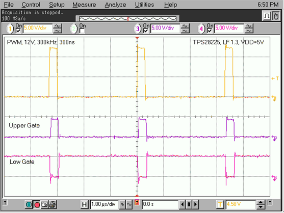 Figure 24. 12-V PWM Pulse at VDD = 5 V
7.3.5 Bootstrap Diode
The bootstrap diode provides the supply voltage for the UGATE driver by charging the bootstrap capacitor connected between BOOT and PHASE pins from the input voltage VDD when the low-side FET is in ON state. At the very initial stage when both power FETs are OFF, the bootstrap capacitor is pre-charged through this path including the PHASE pin, output inductor and large output capacitor down to GND. The forward voltage drop across the diode is only 1.0 V at bias current 100 mA. This allows quick charge restore of the bootstrap capacitor during the high-frequency operation.
7.3.6 Upper and Lower Gate Drivers
The upper and lower gate drivers charge and discharge the input capacitance of the power MOSFETs to allow operation at switching frequencies up to 2 MHz. The output stage consists of a P-channel MOSFET providing source output current and an N-channel MOSFET providing sink current through the output stage. The ON state resistances of these MOSFETs are optimized for the synchronous buck converter configuration working with low duty cycle at the nominal steady state condition. The UGATE output driver is capable of propagating PWM input puses of less than 30-ns while still maintaining proper dead time to avoid any shoot through current conditions. The waveforms related to the narrow input PWM pulse operation are shown in Figure 18.
7.3.7 Dead-Time Control
The dead-time control circuit is critical for highest efficiency and no shoot through current operation throughout the whole duty cycle range with the different power MOSFETs. By sensing the output of driver going low, this circuit does not allow the gate drive output of another driver to go high until the first driver output falls below the specified threshold. This approach to control the dead time is called adaptive. The overall dead time also includes the fixed portion to ensure that overlapping never exists. The typical dead time is around 14 ns, although it varies over the driver internal tolerances, layout and external MOSFET parasitic inductances. The proper dead time is maintained whenever the current through the output inductor of the power stage flows in the forward or reverse direction. Reverse current could happen in a buck configuration during the transients or while dynamically changing the output voltage on the fly, as some microprocessors require. Because the dead time does not depend on inductor current direction, this driver can be used both in buck and boost regulators or in any bridge configuration where the power MOSFETs are switching in a complementary manner. Keeping the dead time at short optimal level boosts efficiency by 1% to 2% depending on the switching frequency. Measured switching waveforms in one of the practical designs show 10-ns dead time for the rising edge of PHASE node and 22 ns for the falling edge (Figure 39 and Figure 40 in the Application Section of the data sheet).
Large non-optimal dead time can cause duty cycle modulation of the DC-to-DC converter during the operation point where the output inductor current changes its direction right before the turn ON of the high-side MOSFET. This modulation can interfere with the controller operation and it impacts the power stage frequency response transfer function. As the result, some output ripple increase can be observed. The TPS28226 driver is designed with the short adaptive dead time having fixed delay portion that eliminates risk of the effective duty cycle modulation at the described boundary condition.
7.3.8 Thermal Shutdown
If the junction temperature exceeds 160°C, the thermal shutdown circuit will pull both gate driver outputs low and thus turning both, low-side and high-side power FETs OFF. When the driver cools down below 140°C after a thermal shutdown, then it resumes its normal operation and follows the PWM input and EN/PG signals from the external control circuit. While in thermal shutdown state, the internal MOSFET pulls the EN/PG pin low, thus setting a flag indicating the driver is not ready to continue normal operation. Normally the driver is located close to the MOSFETs, and this is usually the hottest spots on the PCB. Thus, the thermal shutdown feature of the TPS28226 can be used as an additional protection for the whole system from overheating.
7.4 Device Functional Modes
TPS28226 device functional mode truth table.
Table 1. Truth Table
| PIN | VDD RISING < 3.5 V OR TJ > 160°C |
VDD FALLING > 3 V AND TJ < 150°C | |||
|---|---|---|---|---|---|
| EN/PG RISING < 1.7 V |
EN/PG FALLING > 1.0 V | ||||
| PWM < 1 V | PWM > 1.5 V AND TRISE/TFALL < 200 ns |
PWM SIGNAL SOURCE IMPEDANCE >40 kΩ FOR > 250 ns (3-State)(1) |
|||
| LGATE | Low | Low | High | Low | Low |
| UGATE | Low | Low | Low | High | Low |
| EN/PG | Low | – | – | – | – |