SBVS367A July   2018  – September 2021 TPS3430-Q1

PRODUCTION DATA  

  1. Features
  2. Applications
  3. Description
  4. Revision History
  5. Pin Configuration and Functions
    1.     Pin Functions
  6. Specifications
    1. 6.1 Absolute Maximum Ratings
    2. 6.2 ESD Ratings
    3. 6.3 Recommended Operating Conditions
    4. 6.4 Thermal Information
    5. 6.5 Electrical Characteristics
    6. 6.6 Timing Requirements
    7. 6.7 Timing Diagrams
    8. 6.8 Typical Characteristics
  7. Detailed Description
    1. 7.1 Overview
    2. 7.2 Functional Block Diagrams
    3. 7.3 Feature Description
      1. 7.3.1 CRST
      2. 7.3.2 Window Watchdog
        1. 7.3.2.1 SET0 and SET1
          1. 7.3.2.1.1 Enabling the Window Watchdog
          2. 7.3.2.1.2 Disabling the Watchdog Timer When Using the CRST Capacitor
          3. 7.3.2.1.3 SET0 and SET1 During Normal Watchdog Operation
      3. 7.3.3 Window Watchdog Timer
        1. 7.3.3.1 CWD
        2. 7.3.3.2 WDI Functionality
        3. 7.3.3.3 WDO Functionality
    4. 7.4 Device Functional Modes
      1. 7.4.1 VDD is Below VPOR ( VDD < VPOR)
      2. 7.4.2 VDD is Above VPOR And Below VDD (min)( VPOR < VDD < VDD (min))
      3. 7.4.3 Normal Operation (VDD ≥ VDD (min))
  8. Application and Implementation
    1. 8.1 Application Information
      1. 8.1.1 CRST Delay
        1. 8.1.1.1 Factory-Programmed Watchdog Reset Delay Timing
        2. 8.1.1.2 CRST Programmable Watchdog Reset Delay
      2. 8.1.2 CWD Functionality
        1. 8.1.2.1 Factory-Programmed Timing Options
        2. 8.1.2.2 CWD Adjustable Capacitor Watchdog Timeout
        3. 8.1.2.3 42
    2. 8.2 Typical Applications
      1. 8.2.1 Monitoring Microcontroller with Watchdog Timer - Design 1
        1. 8.2.1.1 Design Requirements - Design 1
        2. 8.2.1.2 Detailed Design Procedure - Design 1
          1. 8.2.1.2.1 Meeting the Minimum Watchdog Reset Delay - Design 1
          2. 8.2.1.2.2 Setting the Watchdog Window - Design 1
          3. 8.2.1.2.3 Calculating the WDO Pull-up Resistor - Design 1
      2. 8.2.2 Monitoring Microcontroller with a Programmed Window Watchdog Timer - Design 2
        1. 8.2.2.1 Design Requirements - Design 2
        2. 8.2.2.2 Detailed Design Procedure - Design 2
          1. 8.2.2.2.1 Meeting the Minimum Watchdog Reset Delay - Design 2
          2. 8.2.2.2.2 Setting the Watchdog Window - Design 2
          3. 8.2.2.2.3 Calculating the WDO Pull-up Resistor - Design 2
      3. 8.2.3 Monitoring Microcontroller with a Latching Window Watchdog Timer - Design 3
        1. 8.2.3.1 Design Requirements - Design 3
        2. 8.2.3.2 Detailed Design Procedure - Design 3
          1. 8.2.3.2.1 Meeting the Latching Output Requirement - Design 3
          2. 8.2.3.2.2 Setting the Watchdog Window - Design 3
        3. 8.2.3.3 Application Curve - Design 3
  9. Power Supply Recommendations
  10. 10Layout
    1. 10.1 Layout Guidelines
    2. 10.2 Layout Example
  11. 11Device and Documentation Support
    1. 11.1 Device Support
    2. 11.2 Documentation Support
      1. 11.2.1 Related Documentation
    3. 11.3 Receiving Notification of Documentation Updates
    4. 11.4 Support Resources
    5. 11.5 Trademarks
    6. 11.6 Electrostatic Discharge Caution
    7. 11.7 Glossary
  12. 12Mechanical, Packaging, and Orderable Information

Package Options

Mechanical Data (Package|Pins)
Thermal pad, mechanical data (Package|Pins)
Orderable Information

Window Watchdog Timer

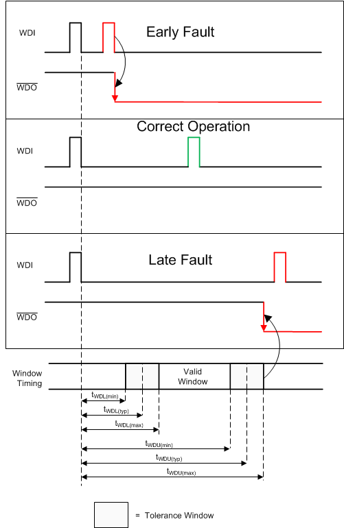
This section provides information for the window watchdog modes of operation. A window watchdog is typically employed in safety critical applications where a traditional watchdog timer is inadequate. In a traditional watchdog, there is a maximum time in which a pulse must be issued to prevent the reset from occurring. However, in a window watchdog the pulse must be issued between a maximum lower window time (tWDL(max)) and the minimum upper window time (tWDU(min)) set by the CWD pin and the SET0 and SET1 pins. Table 8-7 describes how tWDU can be used to calculate the timing of tWDL. The tWDL timing can also be changed by adjusting the SET0 and SET1 pins. Figure 7-5 shows the valid region for a WDI pulse to be issued to prevent the WDO from being triggered and being pulled low.
GUID-BA64609D-18EA-4344-BD1B-FE063105FA97-low.gifFigure 7-5 TPS3430-Q1 Window Watchdog Timing