SBVS187G February   2012  – February 2019 TPS3700

PRODUCTION DATA.  

  1. Features
  2. Applications
  3. Description
    1.     Device Images
      1.      Simplified Schematic
      2.      Output vs Input Thresholds and Hysteresis
  4. Revision History
  5. Pin Configuration and Functions
    1.     Pin Functions
  6. Specifications
    1. 6.1 Absolute Maximum Ratings
    2. 6.2 ESD Ratings
    3. 6.3 Recommended Operating Conditions
    4. 6.4 Thermal Information
    5. 6.5 Electrical Characteristics
    6. 6.6 Timing Requirements
    7. 6.7 Switching Characteristics
    8. 6.8 Typical Characteristics
  7. Detailed Description
    1. 7.1 Overview
    2. 7.2 Functional Block Diagram
    3. 7.3 Feature Description
      1. 7.3.1 Inputs (INA+, INB–)
      2. 7.3.2 Outputs (OUTA, OUTB)
      3. 7.3.3 Window Voltage Detector
      4. 7.3.4 Immunity to Input Terminal Voltage Transients
    4. 7.4 Device Functional Modes
      1. 7.4.1 Normal Operation (VDD > UVLO)
      2. 7.4.2 Undervoltage Lockout (V(POR) < VDD < UVLO)
      3. 7.4.3 Power-On Reset (VDD < V(POR))
  8. Application and Implementation
    1. 8.1 Application Information
      1. 8.1.1 VPULLUP to a Voltage Other Than VDD
      2. 8.1.2 Monitoring VDD
      3. 8.1.3 Monitoring a Voltage Other Than VDD
      4. 8.1.4 Monitoring Overvoltage and Undervoltage for Separate Rails
    2. 8.2 Typical Application
      1. 8.2.1 Design Requirements
      2. 8.2.2 Detailed Design Procedure
        1. 8.2.2.1 Resistor Divider Selection
        2. 8.2.2.2 Pullup Resistor Selection
        3. 8.2.2.3 Input Supply Capacitor
        4. 8.2.2.4 Input Capacitors
      3. 8.2.3 Application Curves
    3. 8.3 Do's and Don'ts
  9. Power-Supply Recommendations
  10. 10Layout
    1. 10.1 Layout Guidelines
    2. 10.2 Layout Example
  11. 11Device and Documentation Support
    1. 11.1 Device Support
      1. 11.1.1 Development Support
        1. 11.1.1.1 Evaluation Modules
      2. 11.1.2 Device Nomenclature
    2. 11.2 Documentation Support
      1. 11.2.1 Related Documentation
    3. 11.3 Receiving Notification of Documentation Updates
    4. 11.4 Community Resources
    5. 11.5 Trademarks
    6. 11.6 Electrostatic Discharge Caution
    7. 11.7 Glossary
  12. 12Mechanical, Packaging, and Orderable Information

Package Options

Refer to the PDF data sheet for device specific package drawings

Mechanical Data (Package|Pins)
  • DSE|6
  • DDC|6
Thermal pad, mechanical data (Package|Pins)
Orderable Information

Monitoring a Voltage Other Than VDD

Some applications monitor rails other than the one that is powering VDD. In these types of applications the resistor divider used to set the desired thresholds is connected to the rail that is being monitored.
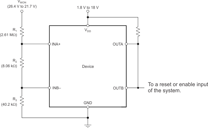
TPS3700 typ_app5_slvsci7.gif

NOTE:

The inputs can monitor a voltage higher than VDDmax with the use of an external resistor divider network.
Figure 18. Monitoring a Voltage Other Than VDD