SBVS344D November   2018  – March 2021 TPS3703-Q1

PRODUCTION DATA  

  1. Features
  2. Applications
  3. Description
  4. Revision History
  5. Device Comparison
  6. Pin Configuration and Functions
  7. Specifications
    1. 7.1 Absolute Maximum Ratings
    2. 7.2 ESD Ratings
    3. 7.3 Recommended Operating Conditions
    4. 7.4 Thermal Information
    5. 7.5 Electrical Characteristics
    6. 7.6 Timing Requirements
    7. 7.7 Timing Diagrams
    8. 7.8 Typical Characteristics
  8. Detailed Description
    1. 8.1 Overview
    2. 8.2 Functional Block Diagram
    3. 8.3 Feature Description
      1. 8.3.1 VDD
      2. 8.3.2 SENSE
      3. 8.3.3 RESET
      4. 8.3.4 Capacitor Time (CT)
      5. 8.3.5 Manual Reset ( MR)
    4. 8.4 Device Functional Modes
      1. 8.4.1 Normal Operation (VDD > VDD(MIN))
      2. 8.4.2 Undervoltage Lockout (VPOR < VDD < UVLO)
      3. 8.4.3 Power-On Reset (VDD < VPOR)
  9. Application and Implementation
    1. 9.1 Application Information
      1. 9.1.1 Voltage Threshold Accuracy
      2. 9.1.2 CT Reset Time Delay
        1. 9.1.2.1 Factory-Programmed Reset Delay Timing
        2. 9.1.2.2 Programmable Reset Delay-Timing
      3. 9.1.3 RESET Latch Mode
      4. 9.1.4 Adjustable Voltage Thresholds
      5. 9.1.5 Immunity to SENSE Pin Voltage Transients
        1. 9.1.5.1 Hysteresis
    2. 9.2 Typical Applications
      1. 9.2.1 Design 1: Multi-Rail Window Monitoring for Microcontroller Power Rails
        1. 9.2.1.1 Design Requirements
        2. 9.2.1.2 Detailed Design Procedure
        3. 9.2.1.3 Application Curves
      2. 9.2.2 Design 2: RESET Latch Mode
        1. 9.2.2.1 Design Requirements
        2. 9.2.2.2 Detailed Design Procedure
        3. 9.2.2.3 Application Curves
  10. 10Power Supply Recommendations
    1. 10.1 Power Supply Guidelines
  11. 11Layout
    1. 11.1 Layout Guidelines
    2. 11.2 Layout Example
  12. 12Device and Documentation Support
    1. 12.1 Device Support
      1. 12.1.1 Device Nomenclature
    2. 12.2 Documentation Support
      1. 12.2.1 Evaluation Module
    3. 12.3 Receiving Notification of Documentation Updates
    4. 12.4 Support Resources
    5. 12.5 Trademarks
    6. 12.6 Electrostatic Discharge Caution
    7. 12.7 Glossary
  13. 13Mechanical, Packaging, and Orderable Information

Package Options

Mechanical Data (Package|Pins)
Thermal pad, mechanical data (Package|Pins)
Orderable Information

Description

The TPS3703-Q1 device is an integrated overvoltage (OV) and undervoltage (UV) monitor or reset IC in industry’s smallest 6-pin DSE package. This highly accurate voltage supervisor is ideal for systems that operate on low-voltage supply rails and have narrow margin supply tolerances. Low threshold hysteresis prevent false reset signals when the monitored voltage supply is in its normal range of operation. Internal glitch immunity and noise filters further eliminate false resets resulting from erroneous signals.

The TPS3703-Q1 does not require any external resistors for setting overvoltage and undervoltage reset thresholds, which further optimizes overall accuracy, cost, solution size, and improves reliability for safety systems. The Capacitor Time (CT) pin is used to select between the two available reset time delays designed into each device and also to adjust the reset time delay by connecting a capacitor. A separate SENSE input pin and VDD pin allow for the redundancy sought by high-reliability systems.

This device has a low typical quiescent current specification of 4.5 µA (typical). The TPS3703-Q1 is suitable for automotive applications and is qualified for AEC-Q100 Grade 1.
Device Information(1)
PART NUMBERPACKAGEBODY SIZE (NOM)
TPS3703-Q1WSON (6)1.50 mm × 1.50 mm
For all available packages, see the orderable addendum at the end of the data sheet.
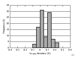
GUID-C084FD53-C357-4E21-A85C-F6C96C4DEA79-low.gif Typical Overvoltage Accuracy Distribution