SBVS149B September 2010 – January 2016 TPS386000-Q1
PRODUCTION DATA.
- 1 Features
- 2 Applications
- 3 Description
- 4 Revision History
- 5 Pin Configuration and Functions
- 6 Specifications
- 7 Parametric Measurement information
- 8 Detailed Description
- 9 Application and Implementation
- 10Power Supply Recommendations
- 11Layout
- 12Device and Documentation Support
- 13Mechanical, Packaging, and Orderable Information
Package Options
Mechanical Data (Package|Pins)
- RGP|20
Thermal pad, mechanical data (Package|Pins)
- RGP|20
Orderable Information
9 Application and Implementation
NOTE
Information in the following applications sections is not part of the TI component specification, and TI does not warrant its accuracy or completeness. TI’s customers are responsible for determining suitability of components for their purposes. Customers should validate and test their design implementation to confirm system functionality.
9.1 Application Information
9.1.1 SENSE Input
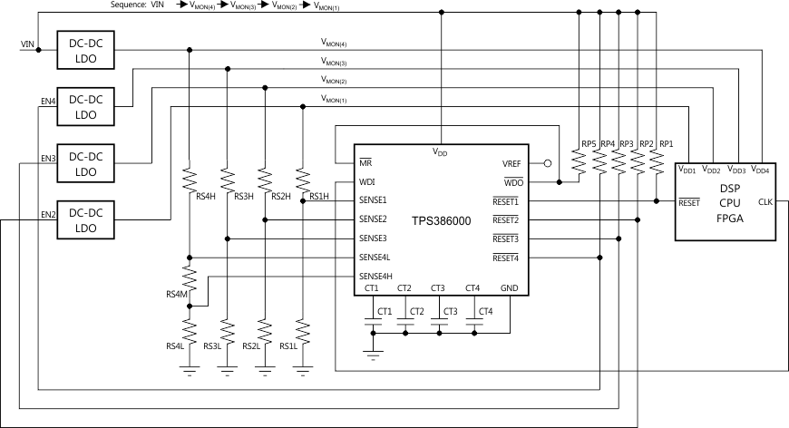
The SENSEm inputs are pins that allow any system voltages to be monitored. If the voltage at the SENSE1, SENSE2, SENSE3, or SENSE4L pins drops below VIT–, then the corresponding reset outputs are asserted. If the voltage at the SENSE4H pin exceeds VIT+, then RESET4 or RESET4 is asserted. The comparators have a built-in hysteresis to ensure smooth reset output assertions and deassertions. Although not required in most cases, for extremely noise applications, it is good analog design practice to place a 1 nF to 10 nF bypass capacitor at the SENSEm input in order to reduce sensitivity to transients, layout parasitics, and interference between power rails monitored by this device. A typical connection of resistor dividers are shown in Figure 31. All the SENSEm pins can be used to monitor voltage rails down to 0.4 V. Threshold voltages can be calculated by following equations:
where
- VDD4_target1 is the undervoltage threshold
where
- VDD4_target2 is the overvoltage threshold
9.1.2 Window Comparator
The comparator at the SENSE4H pin has the opposite comparison polarity to the other SENSEm pins. In the configuration shown in Figure 31, this comparator monitors overvoltage of the VDD4 node; combined with the comparator at SENSE4L, SVS-4 forms a window comparator.
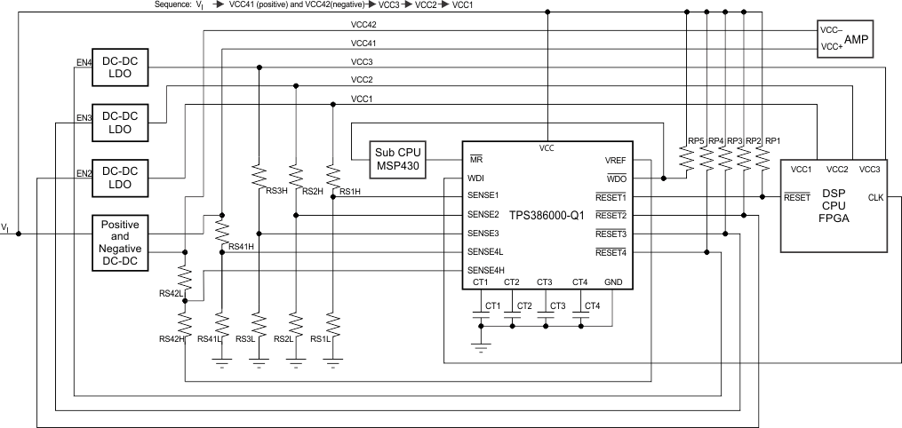
9.1.3 Sensing Voltage Less Than 0.4 V
By using voltage reference output VREF, the SVS-4 comparator can monitor negative voltage or positive voltage lower than 0.4 V. Figure 32 shows this usage in an application circuit. SVS-4 monitors the positive and negative voltage power rail (for example, +15V and –15V supply to an op amp) and the RESET4 or RESET4 output status continues to be as described in Table 4. Note that RS42H is located at higher voltage position than RS42L. The threshold voltage calculations are shown in the following equations:
 Figure 31. Typical Application Circuit (SVS-4: Window Comparator)
9.1.4 Reset Delay Time
Each of the SVS-n channels can be configured independently in one of three modes. Table 6 describes the delay time settings.
Table 6. Delay Timing Selection
| CTn CONNECTION | DELAY TIME |
|---|---|
| Pullup to VDD | 300 ms (typical) |
| Open | 20 ms (typical) |
| Capacitor to GND | Programmable |
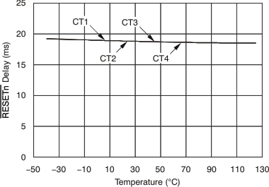
To select the 300-ms fixed delay time, the CTn pin should be pulled up to VDD using a resistor from 40 kΩ to 200 kΩ. Note that there is a pulldown transistor from CTn to GND that turns on every time the device powers on to determine and confirm CTn pin status; therefore, a direct connection of CTn to VDD causes a large current flow. To select the 20-ms fixed delay time, the CTn pin should be left open. To program a user-defined adjustable delay time, an external capacitor must be connected between CTn and GND. The adjustable delay time can be calculated by the following equation:
Using this equation, a delay time can be set to between 1.4 ms to 10 s. The external capacitor should be greater than 220 pF (nominal), so that the TPS386000-Q1 can distinguish it from an open CT pin. The reset delay time is determined by the time it takes an on-chip, precision 300 nA current source to charge the external capacitor to 1.24 V. When the RESETn or RESETn outputs are asserted, the corresponding capacitors are discharged. When the condition to release RESETn or RESETn occurs, the internal current sources are enabled and begin to charge the external capacitors. When the CTn voltage on a capacitor reaches 1.24 V, the corresponding RESETn or RESETn pins are released. Note that a low leakage type capacitor (such as ceramic) should be used, and that stray capacitance around this pin may cause errors in the reset delay time.
9.2 Typical Application
 Figure 32. Application Schematic
9.2.1 Design Requirements
This design is intended to monitor the voltage rails for an FPGA. Table 7 summarizes the design requirements.
Table 7. Design Requirements
| PARAMETER | DESIGN REQUIREMENT |
|---|---|
| VDD | 5 V |
| VMON(1) | 1.8 V –5% |
| VMON(2) | 1.5 V –5% |
| VMON(3) | 1.2 V –5% |
| VMON(4) | 1 V ±5% |
| Approximate start-up time | 100 ms |
9.2.2 Detailed Design Procedure
Select the pullup resistors to be 100 kΩ to ensure that VOL ≤ 0.4 V.
Use Equation 9 to set CT = 22 nF for all channels to obtain an approximate start-up delay of 100 ms.
Select RSnL = 10 kΩ for all channels to ensure DC accuracy.
Use Equation 1 through Equation 6 to determine the values of RSnH and RS4M. Using standard 1% resistors, Table 8 shows the results.
Table 8. Design Results
| RESISTOR | VALUE (kΩ) |
|---|---|
| RS1H | 32.4 |
| RS2H | 25.5 |
| RS3H | 18.7 |
| RS4H | 14.3 |
| RS4M | 1 |
The FPGA does not have a separate watchdog failure input, so a legacy connection is used by connecting WDO to MR.
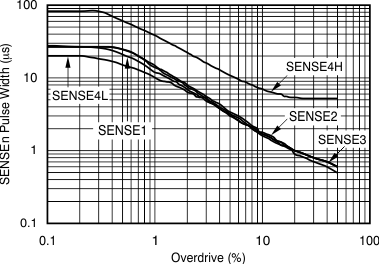
9.2.3 Application Curves


| See Figure 27 for measurement technique |
vs SENSEn Threshold Overdrive Voltage