SBVS172B July 2011 – April 2015
PRODUCTION DATA.
- 1 Features
- 2 Applications
- 3 Description
- 4 Revision History
- 5 Device Comparison Table
- 6 Pin Configuration and Functions
- 7 Specifications
- 8 Detailed Description
- 9 Applications and Implementation
- 10Power Supply Recommendations
- 11Layout
- 12Device and Documentation Support
- 13Mechanical, Packaging, and Orderable Information
Package Options
Mechanical Data (Package|Pins)
- DRY|6
Thermal pad, mechanical data (Package|Pins)
- DRY|6
Orderable Information
1 Features
- Very Small USON (1.45 mm × 1.00 mm) Package
- Adjustable Threshold Down to 500 mV
- Threshold Accuracy: 1% Over Temperature
- Capacitor-Adjustable Delay Time
- Low Quiescent Current: 6 µA (Typical)
- External Enable Input
- Open-Drain (Rated at 18 V) and Push-Pull Output Options
- Temperature Range: –40°C to 125°C
- Pin-for-Pin Compatible With MAX6895/6/7/8
2 Applications
- DSPs, Microcontrollers, and Microprocessors
- Notebook and Desktop Computers
- PDAs and Handheld Products
- Portable and Battery-Powered Products
- FPGAs and ASICs
3 Description
The TPS3895, TPS3896, TPS3897, and TPS3898 devices (TPS389x) are a family of very small supervisory circuits that monitor voltages greater than 500 mV with a 0.25% (typical) threshold accuracy and offer adjustable delay time using external capacitors. The TPS389x family also has a logic enable pin (ENABLE or ENABLE) to power on and off the output. With the TPS3895, for example, when the input voltage pin (SENSE) rises above the threshold, and the ENABLE pin is high, then the output pin (SENSE_OUT) goes high after the capacitor-adjustable delay time. When SENSE falls below the threshold or ENABLE is low, then SENSE_OUT goes low. For truth tables, see Table 1 and Table 2.
For TPS389xA versions, both SENSE and ENABLE have a capacitor-adjustable delay. The output asserts after this capacitor-adjustable delay when both SENSE and ENABLE inputs are good. The TPS389xP devices have a small, 0.2-µs propagation delay from when the enable pin asserts to when the output pin asserts, provided SENSE is above the threshold.
All devices operate from 1.7 V to 6.5 V and have a typical quiescent current of 6 µA with an open-drain output rated at 18 V. The TPS389x is available in an ultra-small USON package and is fully specified over the temperature range of TJ = –40°C to 125°C.
Device Information(1)
| PART NUMBER | PACKAGE | BODY SIZE (NOM) |
|---|---|---|
| TPS389x | USON (6) | 1.45 mm × 1.00 mm |
- For all available packages, see the orderable addendum at the end of the data sheet.
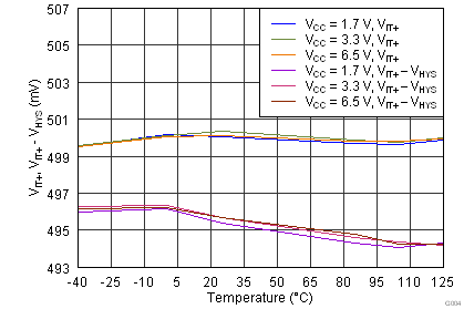
Sense Threshold Voltage vs Temperature
