SLUS930D April 2011 – November 2016 TPS40400
PRODUCTION DATA.
- 1 Features
- 2 Applications
- 3 Description
- 4 Revision History
- 5 Pin Configuration and Functions
- 6 Specifications
-
7 Detailed Description
- 7.1 Overview
- 7.2 Functional Block Diagram
- 7.3
Feature Description
- 7.3.1 Output Voltage Setting
- 7.3.2 Input Voltage Feedforward
- 7.3.3 Output Current Limit and Warning
- 7.3.4 Linear Regulators
- 7.3.5 PMBus Address
- 7.3.6 PMBus Connections
- 7.3.7
PMBus Functionality and Additional Set-Up
- 7.3.7.1 Data Format
- 7.3.7.2 Output Voltage Adjustment
- 7.3.7.3 Overcurrent Threshold
- 7.3.7.4 Output Current Reading
- 7.3.7.5 Soft-Start Time
- 7.3.7.6 Power Good
- 7.3.7.7 Undervoltage Lockout (UVLO)
- 7.3.7.8 Output Overvoltage and Undervoltage Thresholds
- 7.3.7.9 Programmable Fault Responses
- 7.3.7.10 User Data and Adjustable Anti-Cross-Conduction Delay
- 7.4 Device Functional Modes
- 7.5 Programming
- 7.6
Register Maps
- 7.6.1 OPERATION (01h)
- 7.6.2 ON_OFF_CONFIG (02h)
- 7.6.3 CLEAR_FAULTS (03h)
- 7.6.4 WRITE_PROTECT (10h)
- 7.6.5 STORE_DEFAULT_ALL (11h)
- 7.6.6 RESTORE_DEFAULT_ALL (12h)
- 7.6.7 STORE_DEFAULT_CODE (13h)
- 7.6.8 RESTORE_DEFAULT_CODE (14h)
- 7.6.9 VOUT_MODE (20h)
- 7.6.10 VOUT_TRIM (22h)
- 7.6.11 VOUT_MARGIN_HIGH (25h)
- 7.6.12 VOUT_MARGIN_LOW (26h)
- 7.6.13 VOUT_SCALE_LOOP (29h)
- 7.6.14 FREQUENCY_SWITCH (33h)
- 7.6.15 VIN_ON (35h)
- 7.6.16 VIN_OFF (36h)
- 7.6.17 IOUT_CAL_GAIN (38h)
- 7.6.18 IOUT_CAL_OFFSET (39h)
- 7.6.19 VOUT_OV_FAULT_LIMIT (40h)
- 7.6.20 VOUT_OV_FAULT_RESPONSE (41h)
- 7.6.21 VOUT_UV_FAULT_LIMIT (44h)
- 7.6.22 VOUT_UV_FAULT_RESPONSE (45h)
- 7.6.23 IOUT_OC_FAULT_LIMIT (46h)
- 7.6.24 IOUT_OC_FAULT_RESPONSE (47h)
- 7.6.25 IOUT_OC_WARN_LIMIT (4Ah)
- 7.6.26 OT_FAULT_RESPONSE (50h)
- 7.6.27 POWER_GOOD_ON (5Eh)
- 7.6.28 POWER_GOOD_OFF (5Fh)
- 7.6.29 TON_RISE (61h)
- 7.6.30 STATUS_BYTE (78h)
- 7.6.31 STATUS_WORD (78h)
- 7.6.32 STATUS_VOUT (7Ah)
- 7.6.33 STATUS_IOUT (7Bh)
- 7.6.34 STATUS_TEMPERATURE (7Dh)
- 7.6.35 STATUS_CML (7Eh)
- 7.6.36 READ_VIN (88h)
- 7.6.37 READ_VOUT (8Bh)
- 7.6.38 READ_IOUT (8Ch)
- 7.6.39 PMBUS_REVISION (98h)
- 7.6.40 MFR_VIN_MIN (A0h)
- 7.6.41 MFR_VIN_MAX (A1h)
- 7.6.42 MFR_VOUT_MIN (A4h)
- 7.6.43 MFR_VOUT_MAX (A5h)
- 7.6.44 MFR_SPECIFIC_00 (D0h)
- 7.6.45 MFR_SPECIFIC_01 (D1h)
- 7.6.46 MFR_SPECIFIC_02 (D2h)
- 7.6.47 MFR_SPECIFIC_03 (D3h)
- 7.6.48 MFR_SPECIFIC_04 (D4h)
- 7.6.49 MFR_SPECIFIC_05 (D5h)
- 7.6.50 MFR_SPECIFIC_06 (D6h)
- 7.6.51 MFR_SPECIFIC_07 (D7h)
- 7.6.52 MFR_SPECIFIC_44 (FCh)
-
8 Application and Implementation
- 8.1 Application Information
- 8.2
Typical Applications
- 8.2.1
TPS40400 12-V Input, 1.2-V Output, 20-A (maximum) Output Current ConverterAdded Design Example 1
- 8.2.1.1 Design Requirements
- 8.2.1.2
Detailed Design Procedure
- 8.2.1.2.1 Selecting a Switching Frequency
- 8.2.1.2.2 Output Inductor, LOUT
- 8.2.1.2.3 Output Capacitance, COUT
- 8.2.1.2.4 The Resistive Component of Output Ripple
- 8.2.1.2.5 Peak Current Rating of the Inductor
- 8.2.1.2.6 Input Capacitance, CIN
- 8.2.1.2.7 Switching MOSFETs, QHS and QLS
- 8.2.1.2.8 Device Addressing, RADDR0 and RADDR1
- 8.2.1.2.9 Current Sense Flter, R16 and C17
- 8.2.1.2.10 Voltage Decoupling Capacitors, CBP3, CBP6, and CVDD
- 8.2.1.2.11 Bootstrap Capacitor, C9
- 8.2.1.2.12 Snubber R12 and C16
- 8.2.1.2.13 Loop Compensaton Components
- 8.2.1.2.14 Output Voltage Set Point, RBIAS
- 8.2.1.2.15 Remote Sensing
- 8.2.1.3 Application Curves
- 8.2.2 TPS40400 12-V Input 5-V Output, 5-A (Maximum) Output Current Converter Design Example 2Added Design Example 2
- 8.2.1
TPS40400 12-V Input, 1.2-V Output, 20-A (maximum) Output Current ConverterAdded Design Example 1
- 8.3 Initialization Setup
- 9 Power Supply Recommendations
- 10Layout
- 11Device and Documentation Support
- 12Mechanical, Packaging, and Orderable Information
Package Options
Mechanical Data (Package|Pins)
- RHL|24
Thermal pad, mechanical data (Package|Pins)
Orderable Information
6 Specifications
6.1 Absolute Maximum Ratings(1)
| MIN | MAX | UNIT | ||
|---|---|---|---|---|
| Input voltage | VDD | –0.3 | 22 | V |
| SW | –5 | 27 | ||
| BOOT | –0.3 | 30 | ||
| BOOT-SW, HDRV-SW (Differential from BOOT or HDRV to SW) | –0.3 | 7 | ||
| VSNS+, TRACK, SYNC, FB | –0.3 | 7 | ||
| DATA, CLK, CNTL | –0.3 | 3.6 | ||
| ISNS+, ISNS– | –0.3 | 15 | ||
| VSNS– | –0.3 | 0.3 | ||
| Output voltage | HDRV | –0.3 | 30 | V |
| BP3 | –0.3 | 3.8 | ||
| BP6, COMP, PGOOD, DIFFO, LDRV | –0.3 | 7 | ||
| SMBALRT, ADDR0, ADDR1 | –0.3 | 3.6 | ||
| Operating junction temperature, TJ | –40 | 150 | °C | |
| Storage Temperature, Tstg | –55 | 150 | °C | |
(1) Stresses beyond those listed under Absolute Maximum Ratings may cause permanent damage to the device. These are stress ratings only, which do not imply functional operation of the device at these or any other conditions beyond those indicated under Recommended Operating Conditions. Exposure to absolute-maximum-rated conditions for extended periods may affect device reliability.
6.2 ESD Ratings
| VALUE | UNIT | |||
|---|---|---|---|---|
| V(ESD) | Electrostatic discharge | Human body model (HBM), per ANSI/ESDA/JEDEC JS-001(1) | ±2500 | V |
| Charged-device model (CDM), per JEDEC specification JESD22-C101(2) | ±1500 | |||
(1) JEDEC document JEP155 states that 500-V HBM allows safe manufacturing with a standard ESD control process.
(2) JEDEC document JEP157 states that 250-V CDM allows safe manufacturing with a standard ESD control process.
6.3 Recommended Operating Conditions
over operating free-air temperature range (unless otherwise noted)| MIN | MAX | UNIT | ||
|---|---|---|---|---|
| VDD | Controller input voltage | 3 | 20 | V |
| TJ | Operating junction temperature | –40 | 125 | °C |
6.4 Thermal Information
| THERMAL METRIC(1) | TPS40400 | UNIT | |
|---|---|---|---|
| RHL (VQFN) | |||
| 24 PINS | |||
| RθJA | Junction-to-ambient thermal resistance | 31.1 | °C/W |
(1) For more information about traditional and new thermal metrics, see the Semiconductor and IC Package Thermal Metrics application report, SPRA953.
6.5 Electrical Characteristics
Unless otherwise stated, these specifications apply for –40°C ≤ TJ ≤ 125°C, VDD= 12 Vdc, FREQUENCY_SWITCH = 600 kHz| PARAMETER | TEST CONDITIONS | MIN | TYP | MAX | UNIT | |
|---|---|---|---|---|---|---|
| INPUT SUPPLY | ||||||
| VVDD | Input voltage range | 3 | 20 | V | ||
| IVDD | Input operating current | Switching, no driver load | 6 | 15 | mA | |
| VOLTAGE REFERENCE | ||||||
| VFB | Feedback pin voltage default settings | 594 | 600 | 606 | mV | |
| VFB(max) | Feedback pin voltage maximum adjustment | 750 | mV | |||
| VFB(min) | Feedback pin voltage minimum adjustment | 450 | mV | |||
| VFB(inc) | Feedback pin voltage adjustment resolution | 2.34 | mV | |||
| VFB(NL) | Maximum nonlinearity error over adjustment range | 10 | mV | |||
| BP6 REGULATOR | ||||||
| VBP6 | 6-V regulator output voltage | 6.2 | 6.5 | 6.8 | V | |
| VDO6 | Regulator dropout voltage, (VVDD – VBP6) | VVDD = 6 V, IBP6 = 50 mA | 300 | mV | ||
| IBP6 | Regulator current limit | 100 | mA | |||
| BP3 REGULATOR | ||||||
| VBP3 | 3.3-V regulator output voltage | 3.1 | 3.3 | 3.5 | V | |
| VDO3 | Regulator dropout voltage, (VVDD – VBP3) | VVDD = 3 V, IBP3 = 5 mA | 100 | 200 | mV | |
| OSCILLATOR | ||||||
| fSW | Switching frequency | Factory default setting | 480 | 600 | 720 | kHz |
| Nominal frequency range | 200 | 2000 | ||||
| Accuracy | 3 V ≤ VVDD ≤ 20 V, 200 kHz ≤ fSW ≤ 2 MHz | –20% | 20% | |||
| VIH | SYNC high-level input voltage | 2 | V | |||
| VIL | SYNC low-level input voltage | 0.4 | ||||
| ISYNC | SYNC pin leakage current | VSYNC = 6 V | 100 | nA | ||
| VSYNC = 0 V | 100 | |||||
| tSRISE | Maximum SYNC rise time(1) | 100 | ns | |||
| tSYNC | Minimum SYNC pulse width | 100 | ns | |||
| VRMP | Ramp amplitude(1) | FREQUENCY_SWITCH = 200 kHz | VVDD/6.6 | VVDD/6.5 | VVDD/6.3 | V |
| FREQUENCY_SWITCH = 600 kHz | VVDD/7.0 | VVDD/6.8 | VVDD/6.6 | |||
| FREQUENCY_SWITCH = 2000 kHz | VVDD/10 | VVDD/9.6 | VVDD/9.2 | |||
| VVLY | Valley voltage(1) | 0.9 | ||||
| fSYNC | SYNC range % of nominal oscillator frequency | 200 kHz ≤ fSW ≤ 2 MHz | 85% | 150% | ||
| PULSE WIDTH MODULATOR (PWM) | ||||||
| DMAX | Maximum duty cycle(1) (9) | FREQUENCY_SWITCH = 600 kHz | 90% | |||
| FREQUENCY_SWITCH = 1.2 MHz | 85% | |||||
| FREQUENCY_SWITCH = 2 MHz | 75% | |||||
| tOFF(min) | Minimum OFF time | 170 | 225 | ns | ||
| tON(min) | Minimum controllable pulse(1) | TJ = 25°C, fSW = 600 kHz | 75 | ns | ||
| SOFT-START | ||||||
| tSS | Soft-start time(6) | Factory default setting | 2.7 | 3.1 | 3.5 | ms |
| Accuracy | 600 μs ≤ tSS ≤ 9 ms | –15% | 15% | |||
| ERROR AMPLIFIER | ||||||
| GBWP | Gain bandwidth product(1) | 15 | 20 | MHz | ||
| AOL | DC gain(1) | 60 | dB | |||
| IIBFB | Input bias current: FB (out of pin) | 0 | 100 | nA | ||
| IIBT | Input bias current: TRACK (out of pin) | 0 | 250 | nA | ||
| IEAOP | Output source current | VFB = 0 V, VCOMP ≥ 2 V | 1 | mA | ||
| IEAOM | Output sink current | VFB = 2 V, VCOMP ≤ 0.3 V | 1 | |||
| VCOMPH | Error amplifier high output voltage | VFB = 0 V | 3.8 | V | ||
| VCOMPL | Error amplifier low output voltage | VFB = 2 V | 50 | mV | ||
| VTRACK(ofst) | TRACK pin offset voltage | –5 | 5 | mV | ||
| CURRENT SENSE AMPLIFIER | ||||||
| IISNS+ | ISNS+ bias current | 200 | nA | |||
| IISNS– | ISNS– bias current | 100 | μA | |||
| VICM | Input common-mode range | 0.45 | 15 | V | ||
| AOCM | Common-mode gain | –80 | dB | |||
| VLIN | Input linear range, VISNS+ - VISNS-(2) | –45 | 110 | mV | ||
| CURRENT LIMIT PROTECTION | ||||||
| tOFF | Off time between restart attempts | 6 × tSS | ms | |||
| VILIMTH | VCS+ – VCS– voltage that trips OC fault function | Factory default settings(2), TJ = 25°C | 27 | 30 | 33 | mV |
| Threshold accuracy | 3 V ≤ VVDD ≤ 20 V, 30 mV ≤ VILIMTH ≤ 110 mV, TJ = 25°C |
–10% | 10% | |||
| 3V ≤ VVDD ≤ 20 V, VILIMTH ≤ 30 mV, TJ = 25°C |
–3 | 3 | mV | |||
| Comparator offset | VILIMTH = 30 mV, TJ = 25°C | –3 | 3 | mV | ||
| Temperature coefficient(1) | 4000 | ppm/°C | ||||
| tDLYOC | Overcurrent delay | 3-mV overdrive, TJ = 25°C | 155 | ns | ||
| VILIMW | VCS+ – VCS– voltage that sets warning status | Factory default settings, TJ = 25°C | 12 | 15 | 18 | mV |
| Threshold accuracy | 3 V ≤ VVDD ≤ 20V, 1.9 mV ≤ VILIMTH ≤ 120 mV, TJ = 25°C |
–10% | 10% | |||
| 3V ≤ VVDD ≤ 20 V, VILIMTH < 30 mV, TJ = 25°C |
–3 | 3 | mV | |||
| Comparator offset | VILIMTH = 20 mV, TJ = 25°C | –3 | 3 | mV | ||
| Temperature coefficient(1) | 4000 | ppm/°C | ||||
| tDLYOCW | Overcurrent warning delay(1) | 3-mV overdrive | 250 | ns | ||
| BOOTSTRAP | ||||||
| VBOOT | Internal diode voltage drop | IBOOT = 5 mA | 0.7 | 1 | V | |
| IBOOT(lk) | BOOT diode leakage current(1) | (VBOOT – VSW) = 6 V | 1 | μA | ||
| UVLO | ||||||
| VUVLO(on) | VDD UVLO turn on threshold(7) | Factory default settings (minimum) | 2.475 | 2.75 | 3.025 | V |
| Accuracy(7) | 2.25 V ≤ VVDD ≤ 20 V, 2.75 V ≤ VIN_ON ≤ 18 V |
–10% | 10% | |||
| VUVLO(off) | VDD UVLO turnoff threshold(7) | Factory default settings (minimum) | 2.25 | 2.5 | 2.75 | V |
| Accuracy(7) | 2.25 V < VVDD < 20 V, 2.75 V < VIN_OFF < 17.6 V |
–10% | 10% | |||
| REMOTE VOLTAGE SENSE AMPLIFIER | ||||||
| VIOFST | Input offset voltage | –10 | 10 | mV | ||
| RGAIN | Gain-setting resistor(1) | 48 | 60 | 72 | kΩ | |
| VDIFFO | Output voltage at DIFFO pin | VVDD > 6.5 V | 0 | 6 | V | |
| VVDD = 5 V | 0 | 4.5 | ||||
| VVDD = 3 V | 0 | 2.5 | ||||
| KDIFF | Differential gain of amplifier | 0.995 | 1 | 1.005 | V/V | |
| VAGBWP | Closed-loop bandwidth(1) | 2 | MHz | |||
| IVAOP | Output source current | VSNS+ = VDIFFO = 5 V, VSNS– = 0 V | 1 | mA | ||
| IVAOM | Output sink current | VSNS+ = 0 V, VSNS– = 4.5 V, VDIFFO = 5 V | 1 | mA | ||
| POWERGOOD | ||||||
| VPGON | FB pin voltage upper limit for power good on | Factory default settings | 648 | mV | ||
| FB pin voltage lower limit for power good on | 552 | |||||
| Accuracy | 540 mV < VPGON < 660 mV | –5% | 5% | |||
| VPGOFF | FB pin voltage upper limit for power good off | Factory default settings | 660 | mV | ||
| FB pin voltage lower limit for power good off | 540 | |||||
| Accuracy | 528 mV < VPGOFF < 672 mV | –5% | 5% | |||
| RPGD | Pulldown resistance of PGD pin | VFB = 0, IPGOOD = 5 mA | 50 | Ω | ||
| IPGDLK | Leakage current | Factory default settings , 550 mV < VFB < 650 mV, VPGOOD = 5 V |
3 | 15 | μA | |
| tPGD | Delay filter from FB(1) | 5 | μs | |||
| OUTPUT VOLTAGE MARGINING | ||||||
| MRGSLP | VFB slope during margin voltage transition(1) | Factory default settings | 250 | 214 | 188 | V/s |
| Accuracy | 3 V < VVDD < 20 V, 600 μs < tSS < 9 ms | –15% | 15% | |||
| VFBMH | FB pin voltage after margin high command | Factory default settings | 650 | 660 | 670 | mV |
| VFBML | FB pin voltage after margin low command | Factory default settings | 532 | 540 | 548 | mV |
| VFBM(max) | Maximum FB pin voltage with margin | 742 | 750 | 758 | mV | |
| VFBM(min) | Minimum FB pin voltage with margin | 445 | 450 | 455 | mV | |
| VFB(inc) | Resolution of FB steps with margin | 2.34 | mV | |||
| OVERVOLTAGE AND UNDERVOLTAGE DETECTION | ||||||
| VOV | FB pin overvoltage threshold (OV flag) | Factory default settings | 638 | 672 | 705 | mV |
| Accuracy | 3 V < VVDD < 20 V, 648 mV < VOV < 690 mV | –5% | 5% | |||
| VUV | FB pin undervoltage threshold (UV flag) | Factory default settings | 502 | 528 | 554 | mV |
| Accuracy | 3 V < VVDD < 20 V, 510 mV < VOV < 552 mV |
–5% | 5% | |||
| PMBus INTERFACE | ||||||
| VIH | High-level input voltage, CLK, DATA, CNTL | 2.1 | V | |||
| VIL | Low-level input voltage, CLK, DATA, CNTL | 0.8 | V | |||
| IIH | High-level input current, CLK, DATA, CNTL | –10 | 10 | μA | ||
| CNTL | –12 | 10 | ||||
| IIL | Low-level input current, CLK, DATA, CNTL | –10 | 10 | μA | ||
| CNTL | –12 | 10 | ||||
| VOL | Low-level output voltage, DATA, SMBALRT | 3 V ≤ VVDD ≤ 20 V, IOUT = 2 mA | 0.4 | V | ||
| IOH | High-level open-drain leakage current, DATA, SMBALRT | VOUT = 3.6 V | 0 | 10 | μA | |
| CO (1) | Pin capacitance, CLK, DATA | 0.7 | pF | |||
| fPMB | PMBus operating frequency range | Slave mode | 10 | 400 | kHz | |
| PMBus ADDRESSING | ||||||
| IADD | ADDX pin current | 8.23 | 9.75 | 11.21 | μA | |
| VADD(L) | Address pin illegal low voltage threshold | 0.055 | V | |||
| MEASUREMENT SYSTEM | ||||||
| tIDLY | Read delay time(3) | 153 | 192 | 231 | μs | |
| IRES | Current measurement resolution (LSB)(10)(5) | 122 | μV | |||
| IRNG | Current measurement range(5) (4) | –45 | 110 | mV | ||
| IACC | Gain accuracy(8) | –3% | 3% | |||
| IOFST | Offset | –3 | 3 | mV | ||
| VOUT(res) | VOUT measurement resolution (LSB) | 15.625 | mV | |||
| VOUT(rng) | VOUT voltage measurement range | 0 | 14 | V | ||
| VOUT(gain) | Gain accuracy(8)(1) | –2 | 2 | LSB | ||
| VOUT(gain_adj) | Gain adjustment range through PMBus | –10% | 10% | |||
| VOUT(ofst) | Offset(8)(1) | –3% | 3% | |||
| VOUT(ofst_adj) | Gain adjustment range through PMBus | –125 | 124 | mV | ||
| VIN(res) | VIN measurement resolution | 32.5 | mV | |||
| VIN(rng) | VIN voltage measurement range | 3 | 20 | V | ||
| VIN(gain) | Gain accuracy(8)(1) | –2% | 2% | |||
| VIN(gain_adj) | Gain adjustment range through PMBus | –10% | 10% | |||
| VIN(offst) | Offset(8)(1) | –5.5 | –2 | 1.4 | LSB | |
| VIN(offst_adj) | Offset adjustment range through PMBus | –2 | 1.968 | V | ||
| THERMAL SHUTDOWN | ||||||
| TJSD | Junction OT shutdown temperature(1) | 135 | 145 | 155 | °C | |
| TJSDH | Shutdown hysteresis(1) | 25 | 30 | 35 | °C | |
| TJWRN | Junction OT warning threshold(1) | 120 | 130 | 140 | °C | |
| TJWRNH | Junction OT warning temperature hysteresis(1) | 15 | 20 | 25 | °C | |
(1) Specified by design. Not production tested.
(2) The entire current ripple waveform must remain within the linear range for current reading results to be accurate. DC current level must be zero or greater for accurate results. Current sense does not support applications that sink current. Transient voltages (such as ripple) are permitted to fall below 0 V, but must be within the specified linear range.
(3) All read backs are an average of 16 consecutive measurements – not a rolling average. Time is a delay between parameter updates.
(4) Current reading is only supported to 0 average. Voltage transients to –45 mV are taken into account when computing this average.
(5) Voltage is converted to current by dividing by IOUT_CAL_GAIN, the effective value of the resistance used to sense current in the application. Maximum amount that can be reported through PMBus is 64 A.
(6) See Application and Implementation section for more information regarding soft-start time setting.
(7) Although specifications appear to overlap, hysteresis is assured for UVLO turnon and turnoff thresholds.
(8) PMBus commands provide for calibration of each device on an individual basis for improved overall system accuracy.
(9) Operation at 3 V reduces maximum duty cycle by approximately 5%.
(10) Constrained by the resolution of READ_IOUT command. This presents as the greater of 122 µV/ IOUT_CAL_GAIN or 62.5 mA, the resolution of the READ_IOUT command
6.6 Switching Characteristics
over operating free-air temperature range (unless otherwise noted)| PARAMETER | TEST CONDITIONS | MIN | TYP | MAX | UNIT | |
|---|---|---|---|---|---|---|
| RHDHI | High-side driver pullup resistance | (VBOOT – VSW) = 6.4 V, IHDRV = –100 mA, TJ = 25°C |
1.25 | 2.5 | Ω | |
| RHDLO | High-side driver pulldown resistance | (VBOOT – VSW) = 6.4 V, IHDRV = 100 mA, TJ = 25°C |
1.3 | 2.6 | Ω | |
| RLDHI | Low-side driver pullup resistance | TJ = 25°C | 1.25 | 2.5 | Ω | |
| RLDLO | Low-side driver pulldown resistance | TJ = 25°C | 0.8 | 1.5 | Ω | |
| tHRISE | High-side driver rise time(1) | CLOAD = 2.2 nF | 6 | 12.1 | ns | |
| tHFALL | High-side driver fall time(1) | CLOAD = 2.2 nF | 6.3 | 12.6 | ns | |
| tLRISE | Low-side driver rise time(1) | CLOAD = 2.2 nF | 6 | 12.1 | ns | |
| tLFALL | Low-side driver fall time(1) | CLOAD = 2.2 nF | 4 | 8 | ns | |
| tDT | Anti-cross conduction time | MFR_SPECIFIC_00 bit 0 = 0, (short dead time.) |
20 | 50 | ns | |
| ISW | SW pin leakage current (out of pin) | VSW = 0 V | 1 | µA | ||
(1) Specified by Design. Not production tested.
6.7 Dissipation Ratings(1)
| PACKAGE | THERMAL IMPEDANCE JUNCTION-TO-AMBIENT (°C/W) |
AIRFLOW | TA = 25°C POWER RATING (W) |
TA = 85°C POWER RATING (W) |
|---|---|---|---|---|
| 24-Pin Plastic QFN (RHL) |
31.1 | Natural Convection | 3.21 | 1.29 |
| 25.2 | 200 LFM | 3.96 | 1.58 | |
| 23 | 400 LFM | 4.36 | 1.74 |
(1) Ratings based on JEDEC High Thermal Conductivity (High K) Board. For more information on the test method, see TI Technical Brief SZZA017.
6.8 Typical Characteristics
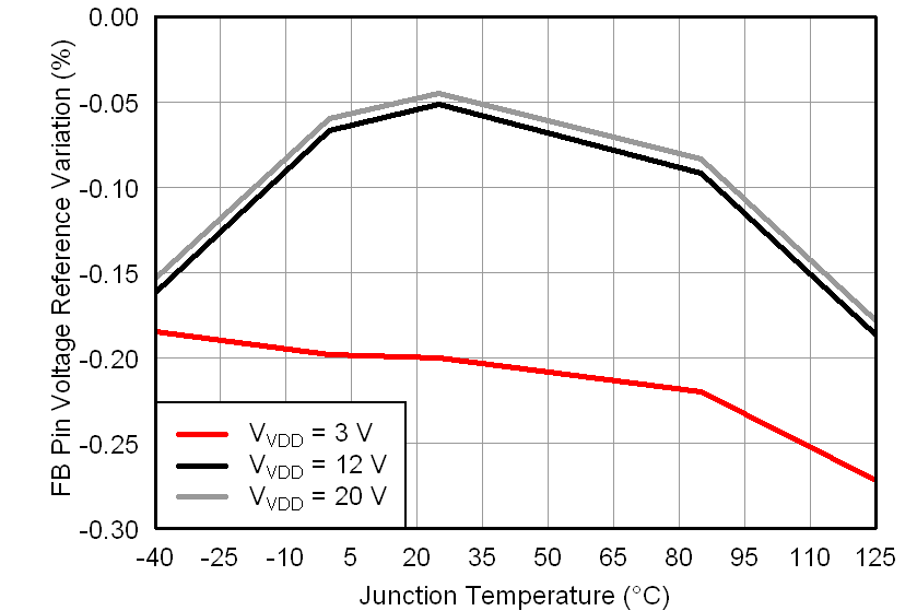 Figure 1. FB Pin Voltage Reference Variation
vs Junction Temperature
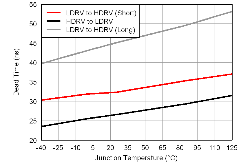 Figure 3. Dead Time
vs. Junction Temperature
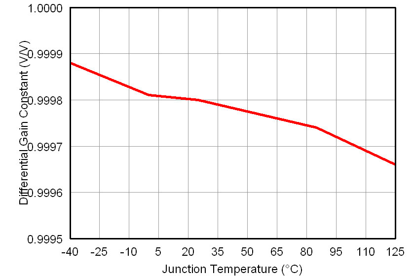 Figure 5. Remote Voltage Amplifier Gain
vs Junction Temperature
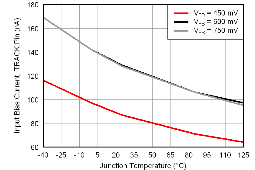 Figure 7. TRACK Pin Input Bias Current
vs Junction Temperature
 Figure 9. Error Amplifier Output Current
vs Junction Temperature
 Figure 11. Low-Side Driver Resistance
vs Junction Temperature
 Figure 13. Switching Frequency Change
vs Junction Temperature
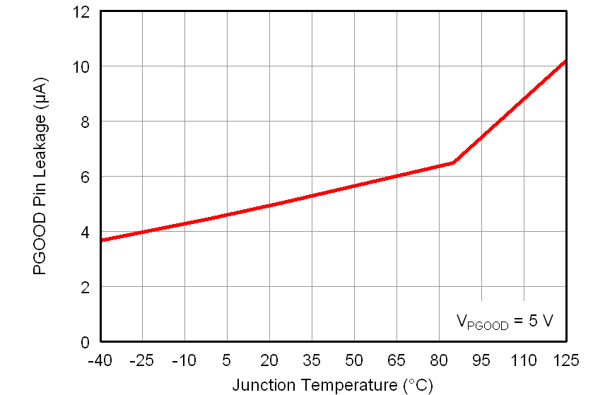 Figure 15. PGOOD Pin Current Leakage
vs Junction Temperature
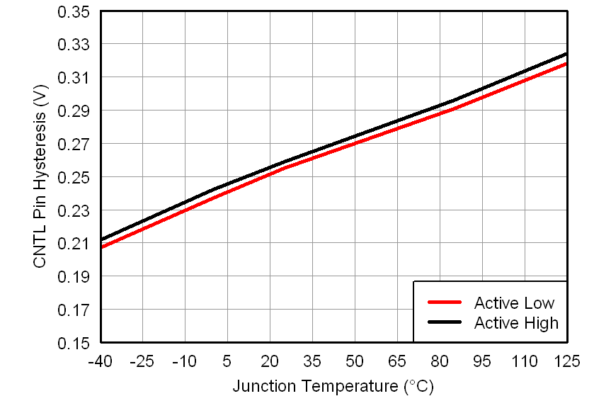 Figure 2. CRTL Pin Hysteresis
vs Junction Temperature
 Figure 4. Remote Voltage Amplifier Offset
 vs Junction Temperature
 Figure 6. TRACK Pin Offset Voltage
vs Junction Temperature
 Figure 8. FB pin Input Bias Current
 vs Junction Temperature
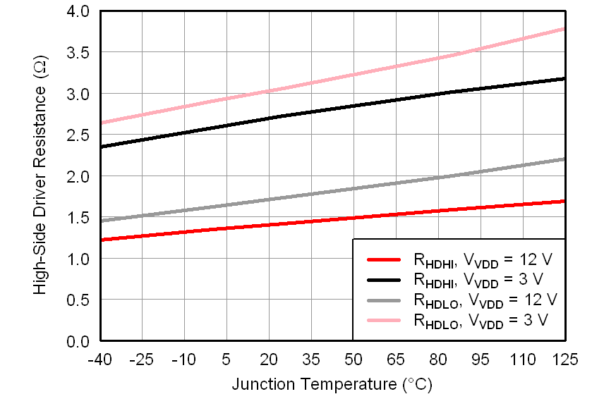 Figure 10. High-Side Driver Resistance
vs Junction Temperature
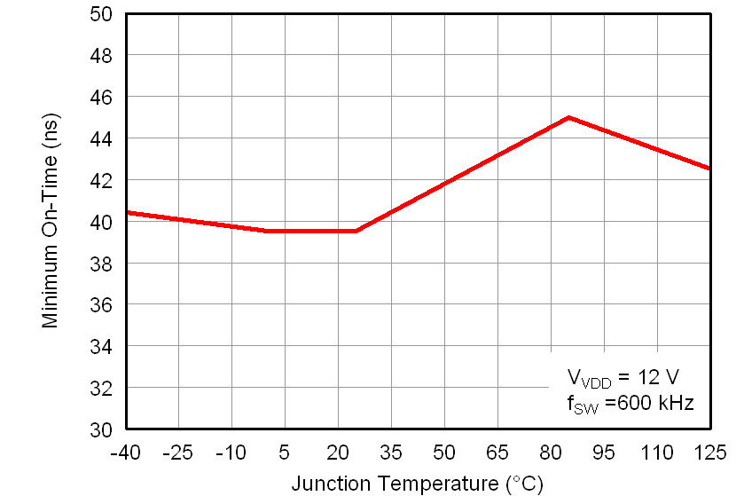 Figure 12. Minimum ON-Time
vs Junction Temperature
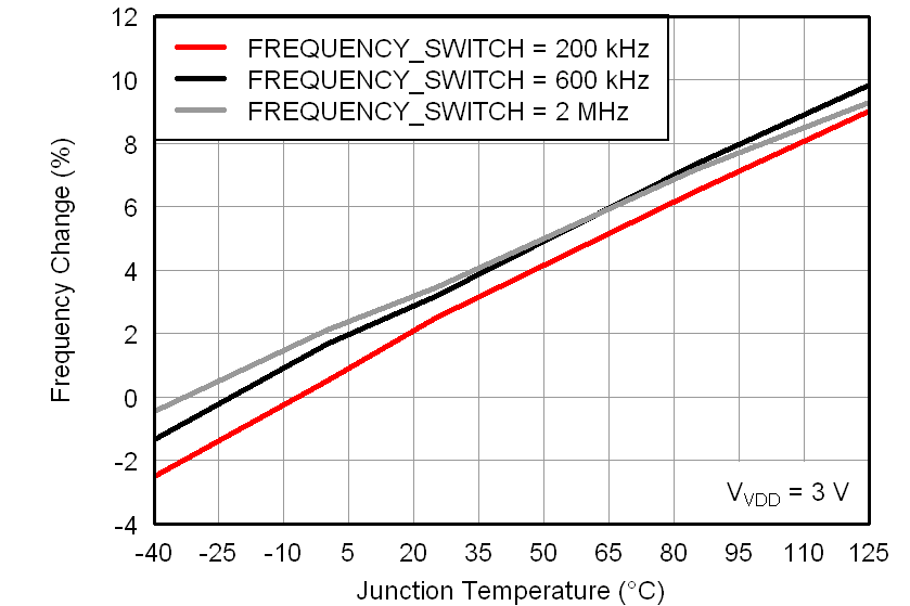 Figure 14. Switching Frequency Change
vs Junction Temperature
 Figure 16. PGOOD Resistance to GND
vs Junction Temperature