SLVSA38B December 2009 – July 2017 TPS43331-Q1
PRODUCTION DATA.
- 1 Features
- 2 Applications
- 3 Description
- 4 Revision History
- 5 Pin Configuration and Functions
-
6 Specifications
- 6.1 Absolute Maximum Ratings
- 6.2 ESD Ratings
- 6.3 Recommended Operating Conditions
- 6.4 Thermal Information
- 6.5 DC Electrical Characteristics
- 6.6 I2C Interface Electrical Characteristics
- 6.7 Switching Regulators Electrical Characteristics
- 6.8 Standby Regulator (VSTBY) Electrical Characteristics
- 6.9 Linear Regulator (VLR) Electrical Characteristics
- 6.10 High-Side Driver (HSD) Electrical Characteristics
- 6.11 AC Switching Characteristics
- 6.12 I2C Interface Switching Characteristics
- 6.13 Switching Regulators Switching Characteristics
- 6.14 Linear Regulator Switching Characteristics
- 6.15 High-Side Driver (HSD) Switching Characteristics
- 6.16 Timing and Switching Diagrams
- 6.17 Typical Characteristics
-
7 Detailed Description
- 7.1 Overview
- 7.2 Functional Block Diagram
- 7.3
Feature Description
- 7.3.1 Unregulated Battery Input Voltage (VBAT)
- 7.3.2 Protected Unregulated Battery Input Voltage (VBATP)
- 7.3.3 Low-Voltage Warning Input (LVWIN)
- 7.3.4 Voltage Warning Output (VBATW)
- 7.3.5 Low-Voltage Reset (RST)
- 7.3.6 Power-Good Delay Timer Input (PGDLY)
- 7.3.7 Active Mode Enable Input (EN)
- 7.3.8 Slew Rate Control Capacitor Input (CSLEW)
- 7.3.9 Charge Pump Capacitor Input (VCP)
- 7.3.10 Power Ground (PGND)
- 7.3.11 Analog Ground Reference (AGND)
- 7.3.12 Inter-IC Communications Interface (I2CID)
- 7.3.13 Clock Input (SCL)
- 7.3.14 Data Line (SDA)
- 7.3.15 Interface Chip Identifier (I2CID)
- 7.3.16 Switch Mode Regulators
- 7.3.17 Upper FET Gate Drive Outputs (VGT1 and VGT2)
- 7.3.18 Lower FET Gate Driver Outputs (VGB1 and VGB2)
- 7.3.19 Bootstrap Capacitor Input (CBS1 and CBS2)
- 7.3.20 Phase Reference for High-Side Bootstrap Supply (PH1 and PH2)
- 7.3.21 Current Sense High-Side (ISHI1 and ISHI2)
- 7.3.22 Current Sense Low-Side (ISLO1 and ISLO2)
- 7.3.23 Regulated Output Sense Voltage Feedback (VFB1 and VFB2)
- 7.3.24 Feedback Compensation Input (VCMP1 and VCMP2)
- 7.3.25 Synchronization Input (SYNCH)
- 7.3.26 Standby Linear Regulator Input (VINSB)
- 7.3.27 Standby Regulator Output (VSTBY)
- 7.3.28 Standby Regulator Sense Voltage (VSTBYS)
- 7.3.29 Switched Linear Regulator Input (VINLR)
- 7.3.30 Switched Linear Regulator Output (VLR)
- 7.3.31 Switched Linear Regulator Sense Voltage (VLRS)
- 7.3.32 High-Side Driver Output (HSD)
- 7.4 Device Functional Modes
- 7.5 Programming
- 7.6 Register Map
-
8 Application and Implementation
- 8.1 Application Information
- 8.2 Typical Application
- 8.3 System Example
- 9 Power Supply Recommendations
- 10Layout
- 11Device and Documentation Support
- 12Mechanical, Packaging, and Orderable Information
Package Options
Mechanical Data (Package|Pins)
- DAP|38
Thermal pad, mechanical data (Package|Pins)
- DAP|38
Orderable Information
1 Features
- Qualified for Automotive Applications
- AEC-Q100 Qualified With the Following Results:
- Input Operating Range 5 V to 30 V (VBAT)
- Two, Adjustable Output Voltage, Step-Down Switching Voltage Regulators
- External Clock Input
- Soft-Start Control for Step-Down Regulators
- Programmable, Linear Regulator (VSTBY), Low Quiescent Current (65 µA typ)
- Programmable, Linear Regulator (VLR)
- Overvoltage Detection and Shutdown
- Protected, High-Side Drive Ouput (HSD)
- Power-On Reset for Standby Regulator (VSTBY)
- Serial Communication, I2C Interface
- Low Voltage Warning Detection With Programmable Input Threshold (LVWIN, VBATW)
- Enable Feature, Controls VBUCK 1
- Programmable Power Good Delay Time (PGDLY) for VSTBY
- Current-Limit and Independent Thermal Detection and Shutdown Protection on All Regulators and High-Side Driver Output
- Thermally Enhanced 38-Pin DAP PowerPAD™ Package
2 Applications
- Automotive Applications
- Power Supply for Microcontrollers and DSPs
3 Description
The TPS43331-Q1 is a multi-rail output voltage regulator, with two synchronous switch mode controllers and two linear regulators. In addition, there is a reverse protected high side switch and voltage supervisor for monitoring the standby regulator and input voltage. The regulator outputs and high side switch are controlled either by discrete inputs for certain outputs and serial interface using the I2C configuration for outputs not controlled by discrete inputs.
The standby linear regulator (VSTBY) is high voltage tolerant and can be connected directly to the vehicle battery, the quiescent current is typically 65 µA to maintain a regulated output with light loads.
Device Information(1)
| PART NUMBER | PACKAGE | BODY SIZE (NOM) |
|---|---|---|
| TPS43331-Q1 | HTSSOP (38) | 12.50 mm × 6.10 mm |
- For all available packages, see the orderable addendum at the end of the data sheet.
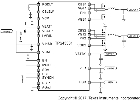
Simplified Schematic

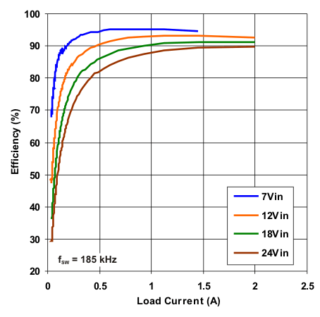
Efficiency vs Load Current (VOUT = 5 V)
