SLVSA38B December 2009 – July 2017 TPS43331-Q1
PRODUCTION DATA.
- 1 Features
- 2 Applications
- 3 Description
- 4 Revision History
- 5 Pin Configuration and Functions
-
6 Specifications
- 6.1 Absolute Maximum Ratings
- 6.2 ESD Ratings
- 6.3 Recommended Operating Conditions
- 6.4 Thermal Information
- 6.5 DC Electrical Characteristics
- 6.6 I2C Interface Electrical Characteristics
- 6.7 Switching Regulators Electrical Characteristics
- 6.8 Standby Regulator (VSTBY) Electrical Characteristics
- 6.9 Linear Regulator (VLR) Electrical Characteristics
- 6.10 High-Side Driver (HSD) Electrical Characteristics
- 6.11 AC Switching Characteristics
- 6.12 I2C Interface Switching Characteristics
- 6.13 Switching Regulators Switching Characteristics
- 6.14 Linear Regulator Switching Characteristics
- 6.15 High-Side Driver (HSD) Switching Characteristics
- 6.16 Timing and Switching Diagrams
- 6.17 Typical Characteristics
-
7 Detailed Description
- 7.1 Overview
- 7.2 Functional Block Diagram
- 7.3
Feature Description
- 7.3.1 Unregulated Battery Input Voltage (VBAT)
- 7.3.2 Protected Unregulated Battery Input Voltage (VBATP)
- 7.3.3 Low-Voltage Warning Input (LVWIN)
- 7.3.4 Voltage Warning Output (VBATW)
- 7.3.5 Low-Voltage Reset (RST)
- 7.3.6 Power-Good Delay Timer Input (PGDLY)
- 7.3.7 Active Mode Enable Input (EN)
- 7.3.8 Slew Rate Control Capacitor Input (CSLEW)
- 7.3.9 Charge Pump Capacitor Input (VCP)
- 7.3.10 Power Ground (PGND)
- 7.3.11 Analog Ground Reference (AGND)
- 7.3.12 Inter-IC Communications Interface (I2CID)
- 7.3.13 Clock Input (SCL)
- 7.3.14 Data Line (SDA)
- 7.3.15 Interface Chip Identifier (I2CID)
- 7.3.16 Switch Mode Regulators
- 7.3.17 Upper FET Gate Drive Outputs (VGT1 and VGT2)
- 7.3.18 Lower FET Gate Driver Outputs (VGB1 and VGB2)
- 7.3.19 Bootstrap Capacitor Input (CBS1 and CBS2)
- 7.3.20 Phase Reference for High-Side Bootstrap Supply (PH1 and PH2)
- 7.3.21 Current Sense High-Side (ISHI1 and ISHI2)
- 7.3.22 Current Sense Low-Side (ISLO1 and ISLO2)
- 7.3.23 Regulated Output Sense Voltage Feedback (VFB1 and VFB2)
- 7.3.24 Feedback Compensation Input (VCMP1 and VCMP2)
- 7.3.25 Synchronization Input (SYNCH)
- 7.3.26 Standby Linear Regulator Input (VINSB)
- 7.3.27 Standby Regulator Output (VSTBY)
- 7.3.28 Standby Regulator Sense Voltage (VSTBYS)
- 7.3.29 Switched Linear Regulator Input (VINLR)
- 7.3.30 Switched Linear Regulator Output (VLR)
- 7.3.31 Switched Linear Regulator Sense Voltage (VLRS)
- 7.3.32 High-Side Driver Output (HSD)
- 7.4 Device Functional Modes
- 7.5 Programming
- 7.6 Register Map
-
8 Application and Implementation
- 8.1 Application Information
- 8.2 Typical Application
- 8.3 System Example
- 9 Power Supply Recommendations
- 10Layout
- 11Device and Documentation Support
- 12Mechanical, Packaging, and Orderable Information
Package Options
Mechanical Data (Package|Pins)
- DAP|38
Thermal pad, mechanical data (Package|Pins)
- DAP|38
Orderable Information
6 Specifications
6.1 Absolute Maximum Ratings
over operating free-air temperature range (unless otherwise noted)(1)(2)| MIN | MAX | UNIT | ||
|---|---|---|---|---|
| Unregulated input(3) | VBAT, VBATP | –0.3 | 40 | V |
| Unregulated power supply(3) | VINSB, VINLR | –0.3 | 40 | V |
| High side output(4) | HSD | –0.3 | 40 | V |
| Low voltage warning input | LVWIN | –0.3 | 40 | V |
| Switched linear regulator | VLR | –0.3 | 15 | V |
| Bootstrap capacitor | VCP | –0.3 | 18 | V |
| Logic level or low voltage signals | PGDLY, CSLEW, VBATW, RST, EN, VSTBYS, VSTBY, VLRS, SYNCH, I2CID, SCL, SDA, VCMP1, VCMP2, VFB1, VFB2(3) | –0.3 | 5.5 | V |
| ISHI1, ISHI2, ISLO1, ISLO2(3) | –0.3 | 10 | ||
| CBS1, CBS2, VGT1, VGT2 | –0.3 | 40 | ||
| VGB1, VGB2 | –0.3 | 10 | ||
| PH1, PH2(4) | –1 | 40 | ||
| Operating junction temperature range, TJ | –40 | 150 | °C | |
| Storage temperature range, Tstg | –65 | 150 | °C | |
(1) Stresses beyond those listed under Absolute Maximum Ratings may cause permanent damage to the device. These are stress ratings only, and functional operation of the device at these or any other conditions beyond those indicated under Recommended Operating Conditions is not implied. Exposure to absolute-maximum-rated conditions for extended periods may affect device reliability.
(2) All voltage values are with respect to GND.
(3) Absolute negative voltage on these pins not to go below –0.5 V.
(4) Absolute negative voltage on these pins not to go below –1 V, and transients of –2 V because of recirculation of an inductive load
for < 100 ns.
for < 100 ns.
6.2 ESD Ratings
| VALUE | UNIT | |||
|---|---|---|---|---|
| V(ESD) | Electrostatic discharge | Human-body model (HBM), per AEC Q100-002(1) | 2000 | V |
(1) AEC Q100-002 indicates that HBM stressing shall be in accordance with the ANSI/ESDA/JEDEC JS-001 specification.
6.3 Recommended Operating Conditions
| MIN | MAX | UNIT | |||
|---|---|---|---|---|---|
| Unregulated input | VBAT, VBATP | 5 | 30 | V | |
| Unregulated power supply | VINSB, VINLR | 1.8 | 30 | V | |
| High side output | HSD | 5 | 30 | V | |
| Low voltage warning input | LVWIN | 5 | 30 | V | |
| Linear regulator | VLR | 1.2 | 12 | V | |
| Standby regulator | VSTBY, VSTBYS | 1.2 | 5 | V | |
| Bootstrap capacitor | VCP | 16 | V | ||
| Logic level or low voltage signals | PGDLY, CSLEW, VBATW, RST, EN, VLRS, SYNCH, I2CID, SCL, SDA, VCMP1, VCMP2, VFB1, VFB2 | 4.5 | 5.3 | V | |
| ISHI1, ISHI2, ISLO1, ISLO2 | 1.2 | 9 | V | ||
| CBS1, CBS2, VGT1, VGT2 | 5 | 38 | V | ||
| VGB1, VGB2 | 3 | 8 | V | ||
| PH1, PH2 | –1 | 30 | V | ||
| TA | Operating ambient temperature(1) | –40 | 125 | °C | |
(1) Assumes TA = TJ – Power dissipation × θJA
6.4 Thermal Information
| THERMAL METRIC(1) | TPS43331-Q1 | UNIT | |
|---|---|---|---|
| DAP (HTSSOP) | |||
| 38 PINS | |||
| RθJA | Junction-to-ambient thermal resistance(2) | 25 | °C/W |
| RθJC(top) | Junction-to-case (top) thermal resistance(3) | 10 | °C/W |
| RθJB | Junction-to-board thermal resistance | — | °C/W |
| ψJT | Junction-to-top characterization parameter | — | °C/W |
| ψJB | Junction-to-board characterization parameter | — | °C/W |
| RθJC(bot) | Junction-to-case (bottom) thermal resistance | — | °C/W |
(1) For more information about traditional and new thermal metrics, see the Semiconductor and IC Package Thermal Metrics application report.
(2) This assumes a JEDEC JESD 51-5 standard board with thermal vias – See the Layout Example section and the application report PowerPAD Thermally Enhanced Package for more information.
(3) This assumes junction to exposed thermal pad.
6.5 DC Electrical Characteristics
VBAT = VBATP = 6 V to 18 V, TJ = –40°C to +150ºC (unless otherwise noted)6.6 I2C Interface Electrical Characteristics
VBAT = VBATP = 6 V to 18 V, TJ = –40°C to +150ºC (unless otherwise noted)| PARAMETER | TEST CONDITIONS | MIN | TYP | MAX | UNIT | |
|---|---|---|---|---|---|---|
| I2CID Serial interface ID address input | ||||||
| VIH | Input high threshold | 2 | V | |||
| VIL | Input low threshold | 0.8 | V | |||
| VHYS | Hysteresis | 0.3 | 0.8 | V | ||
| ILKG | Input leakage current | I2CID = 3.3 V | –1 | 1 | µA | |
| SCL Serial clock input for synchronization | ||||||
| VIH | Input high threshold | 2 | V | |||
| VIL | Input low threshold | 0.8 | V | |||
| VHYS | Hysteresis | 0.3 | 0.8 | V | ||
| ILKG | Input leakage current | 0.3 V ≤ VSCL ≤ 3.0 V | –1 | 1 | µA | |
| CSCLIN | Input line capacitance | 10 | pF | |||
| SDA Serial communications data line | ||||||
| VIH | Input high threshold | 2 | V | |||
| VIL | input low threshold | 0.8 | V | |||
| VHYS | Hysteresis | 0.3 | 0.8 | V | ||
| ILeakage | Leakage current | 0.3 V ≤ VSDA ≤ 3.0 V | –1 | 1 | µA | |
| VSAT | Output saturation voltage | IOL = 3 mA | 0.4 | V | ||
| IOL = 6 mA | 0.6 | V | ||||
| CSDAIN | Input line capacitance | 10 | pF | |||
6.7 Switching Regulators Electrical Characteristics
VBAT = VBATP = 6 V to 18 V, TJ = –40°C to +150ºC (unless otherwise noted)| PARAMETER | TEST CONDITIONS | MIN | TYP | MAX | UNIT | |
|---|---|---|---|---|---|---|
| Switch mode regulators (Channel 1) | ||||||
| IO | Output current | 4 | A | |||
| VO | Regulated output voltage range | 1.2 | 10 | V | ||
| VFB1 | Feedback voltage input | 980 | 1020 | mV | ||
| VOTOL | Regulated output voltage tolerance | IO = 100% to 10% IO(max), Includes external feedback resistors | –5% | 5% | ||
| VISCTH | Short circuit current, voltage threshold(1) | 60 | 120 | mV | ||
| VDO | Dropout voltage(2) | IO = IO(max), VBAT = 9 V, Includes drop due to VISCTH | 400 | mV | ||
| dV/dt | Output voltage soft-start slew rate(3) | Step response on regulator enable, IO = IO(max) | 10 | V/ms | ||
| 5% | ||||||
| VP_SC | Overshoot (4) | IO = ISC(max), Remove short | 5% | |||
| VP_TR | Load transient response(4) | IO = 10% to 100% IO(max) | –5% | |||
| IO = 100% to 10% IO(max) | 5% | |||||
| IVGT1_SRC | Gate drive source current (high side) | VGT1 = VGB1 = 6 V, Measure time calculate current | 210 | 330 | mA | |
| IVGT1_SINK | Gate drive sink current (high side) | VGT1 = VGB1 = 6 V, Measure time calculate current | 500 | 1020 | mA | |
| IVGB1_SRC | Gate drive source current (low side) | VGT1 = VGB1 = 6 V, Measure time calculate current | 90 | 135 | mA | |
| IVGB1_SINK | Gate drive sink current (low side) | VGT1 = VGB1 = 6 V, Measure time calculate current | 440 | 1300 | mA | |
| Switch mode regulators (Channel 2), SW2EN = 1 (unless otherwise noted) | ||||||
| IO | Output current | 4.0 | A | |||
| VO | Regulated output voltage range | 1.2 | 10 | V | ||
| VFB1 | Feedback voltage input | 980 | 1020 | mV | ||
| VOTOL | Regulated output voltage tolerance | IO = 100% to 10% IO(max), Includes external feedback resistors | –5% | 5% | ||
| VISCTH | Short circuit current, voltage threshold(1) | 60 | 120 | mV | ||
| VDO | Dropout voltage(2) | IO = IO(max), VBAT = 9 V, Includes drop due to VISCTH | 400 | mV | ||
| dV/dt | Output voltage soft-start slew rate(3) | Step response on regulator enable, IO = IO(max) | 10 | V/ms | ||
| VP_SC | Overshoot(4) | IO = ISC(max), Remove short | 5% | |||
| VP_TR | Load transient response(4) | IO = 10% to 100% IO(max) | –5% | |||
| IO = 100% to 10% IO(max) | 5% | |||||
| IVGT2_SRC | Gate drive source current (high side) | VGT1 = VGB1 = 6 V, Measure time calculate current | 210 | 330 | mA | |
| IVGT2_SINK | Gate drive sink current (high side) | VGT1 = VGB1 = 6 V, Measure time calculate current | 500 | 1020 | mA | |
| IVGB2_SRC | Gate drive source current (low side) | VGT1 = VGB1 = 6 V, Measure time calculate current | 90 | 135 | mA | |
| IVGB2_SINK | Gate drive sink current (low side) | VGT1 = VGB1 = 6 V, Measure time calculate current | 440 | 1300 | mA | |
(1) The output remains stable using soft-start conditions when the output drops from regulation to 0 V. The device is not damaged by a hard short to ground.
(2) Lower VBAT until the output drops to 0.1 V. Measure VBAT – VO.
(3) Design information – Not tested. Specified by CSLEW current and bench characterization.
(4) Design information – Not tested.
6.8 Standby Regulator (VSTBY) Electrical Characteristics
VINLR = 3 V to 18 V, VBAT = VBATP = 6 V to 18 V, TJ = –40°C to +150ºC (unless otherwise noted)| PARAMETER | TEST CONDITIONS | MIN | TYP | MAX | UNIT | |
|---|---|---|---|---|---|---|
| IO | Output current | Active mode | 5 | 300 | mA | |
| Standby mode | 0.05 | 300 | ||||
| VO | Regulated output voltage range | VINSB = (VO + VDO) to 18 V, IO = IO(max)(2) to IO(min), TA = –40°C to +50°C, VINSB = 18 V to 26.5 V, IO = IO(max)(3) to IO(min) |
1.2 | 3.6 | V | |
| VSTBYS | Feedback input voltage for standby regulator | 980 | 1020 | mV | ||
| VSTBY | Regulated output voltage tolerance | IO = IO(max) to IO(min), VO + VDO < VINSB < 18 V, 1% nominal (3% worse case) tolerance resistors |
–5% | 5% | ||
| IO = IO(max) to IO(min), 18 V < VINSB < 26.5 V | 8% | |||||
| LR | Load regulation | IO = IO(max) to IO(min) | –4% | 0% | ||
| SR | Line regulation | IO = IO(max), VO + VDO < VINSB < 18 V | –4% | 4% | ||
| ISC | Short circuit current limit | VSTBY = 0 V(4) | 310 | 1400 | mA | |
| VDO | Dropout voltage(2) | IO = 300 mA | 1200 | mV | ||
| VLVRTH | Low-voltage reset threshold | Lower VO until goes low | 900 | 950 | mV | |
| TSD | Thermal shutdown(1) | 150 | 210 | °C | ||
| THYS | Hysteresis | 5 | 15 | °C | ||
| ΔV/ΔT | Output voltage slew rate(3) | Step response on regulator, IO = IO(min) | 10 | V/mS | ||
| VOP_SC | Overshoot(1) | IO = ISC(min), Remove short | 5% | |||
| VP_TR | Load transient response (1) | Active mode, VSTBY = 1.2 V, CVSTBY = 1 µF, Δt = 10 µs, IO = IO(min) to IO(max), IO = IO(max) to IO(min) |
–6% | 6% | ||
| Active mode, VSTBY = 3.6 V, CVSTBY = 1 µF, Δt = 10 µs, IO = IO(min) to IO(max), IO = IO(max) to IO(min) |
–6% | 6% | ||||
| Standby mode, VSTBY = 1.2 V, CVSTBY = 1 µF, Δt = 10 µs, IO = –100 mA to IO(max), IO = IO(max) to –100 mA |
–6% | 6% | ||||
| Standby mode, VSTBY = 3.6 V, CVSTBY = 1 µF, Δt = 10 µs, IO = –100 mA to IO(max), IO = IO(max) to –100 mA |
–6% | 6% | ||||
| VPRSS | Power supply rejection ratio(1) | IO = 0.5×IO(max), fo = 120 Hz to 10 kHz, VINSB = 14-V DC and 1-V AC (p – p) | 50 | dB | ||
| IO = 0.5×IO(max), fo = 20 to 20 kHz, VINSB = 14-V DC and 1-V AC (p – p) | 45 | |||||
| VN | Output noise | 100-kHz low-pass filter, fo = 20 Hz to 100 kHz, IVSTBY = –5 mA | 400 | uV | ||
| 100-kHz low-pass filter, fo = 20 Hz to 20 kHz, IVSTBY = –5 mA | 200 | |||||
| ttr | Output voltage transient response | IO = IO(min) to IO(max), CO(max) | 40 | µs | ||
| CO | Output capacitance | CO(nom) = 1 µF, 16 V | 0.53 | 1.15 | µF | |
| RESR | Output capacitance ESR | f = 1 kHz, TA = 125°C | 8.75 | Ω | ||
| DF | Output capacitor dissipation factor | f = 1 kHz, TA = –40°C | 1% | |||
| f = 1 kHz, TA = 25°C | 3.5% | |||||
| f = 1 kHz, TA = 125°C | 5.5% | |||||
(1) Design information – Not tested.
(2) This nomenclature is meant to agree with the convention that current flow into the pin is a positive. Therefore Io(max) is a smaller magnitude current and Io(min) is larger magnitude current throughout the parametric tables.
(3) Design information – Not tested, parameter assured by characterization.
(4) The output remains stable using soft-start conditions when the output drops from regulation to 0 V. The IC is not damaged by a hard short to ground.
6.9 Linear Regulator (VLR) Electrical Characteristics
VINLR = 3 V to 18 V, VBAT = VBATP = 6 V to 18 V, TJ = –40°C to +150ºC (unless otherwise noted)| PARAMETER | TEST CONDITIONS | MIN | TYP | MAX | UNIT | |
|---|---|---|---|---|---|---|
| IO | Output current | 5 | 650 | mA | ||
| VO | Regulated output voltage range | VINLR = (VO + VDO) to 18 V, IO = IO(max) to IO(min), TA = –40°C to +50°C, VINLR = 18 V to 26.5 V, IO = IO(max) to IO(min) |
1.2 | 8.5 | V | |
| VLRS | Feedback input voltage | 980 | 1020 | mV | ||
| VLR | Output voltage tolerance | IO = IO(max) to IO(min), VO + VDO < VINLR < 18 V, 1% nominal (3% worse case) tolerance resistors |
–5% | 5% | ||
| IO = IO(max) to IO(min), VINLR = 18 V to 26.5 V | 8% | |||||
| LR | Load regulation | IO = IO(max) to IO(min) | –4% | 1% | ||
| SR | Line regulation | IO = IO(max), VO + VDO < VINLR < 18 V | –4% | 4% | ||
| IO = IO(max), 18 V < VINLR < 26.5 V | –4% | 4% | ||||
| ISC | Short circuit current limit | VLR = 0 V(4) | 0.7 | 2.7 | A | |
| VDO | Dropout voltage(2) | IO = –200 mA | 400 | mV | ||
| IO = –600 mA | 1.7 | V | ||||
| TSD | Thermal shutdown(1) | 150 | 210 | ºC | ||
| THYS | Hysteresis | 5 | 15 | ºC | ||
| VOP_SC | Overshoot | IO = ISC(min), Remove short | 5% | |||
| VP_TR | Load transient response(1) | VLR =1.2 V, CVLR = 1 µF, Δt = 10 µs, IO = IO(min) to IO(max), IO = IO(max) to IO(min) |
–6% | 6% | ||
| VLR = 8.5 V, CVLR = 1 µF, Δt = 10 µs, IO = IO(min) to IO(max), IO = IO(max) to IO(min) |
–6% | 6% | ||||
| VPRSS | Power supply rejection ratio(1) | IO = 0.5×IO(max), fo = 120 Hz to 10 kHz, VINLR = 14-V DC and 1-V AC (p – p) |
50 | dB | ||
| IO = 0.5×IO(max), fo = 20 Hz to 20 kHz, VINLR = 14-V DC and 1-V AC (p – p) |
45 | |||||
| VN | Output noise(1) | 100-kHz low-pass filter, fo = 20 Hz to 100 kHz, IVLR = –5 mA | 400 | uV | ||
| Weighted filter, fo = 20 Hz to 20 kHz, IVLR = –5 mA | 200 | |||||
| ttr | Output voltage transient response(1) | IO = IO(min) to IO(max), CO(max) | 40 | µs | ||
| CO | Output capacitance(1) | CO(nom) = 1 µF, 16 V | 0.53 | 1.15 | µF | |
| RESR | Output capacitance ESR(1) | f = 1 kHz, TA = 125°C | 8.75 | Ω | ||
| DF | Output capacitor dissipation factor(1) | f = 1 kHz, TA = –40°C | 1% | |||
| f = 1 kHz, TA = 25°C | 3.5% | |||||
| f = 1 kHz, TA = 125°C | 5.5% | |||||
(1) Design information – Not tested
6.10 High-Side Driver (HSD) Electrical Characteristics
VBAT = VBATP = 6 V to 18 V, HSD1EN = 1, TJ = –40°C to +150ºC (unless otherwise noted)| PARAMETER | TEST CONDITIONS | MIN | TYP | MAX | UNIT | |
|---|---|---|---|---|---|---|
| VSAT | HSD output saturation voltage | IHSD = –300 mA | 0.6 | V | ||
| IHSD = –450 mA, t = 0.5 s | 1.2 | V | ||||
| ILKG | Leakage current | HSD1EN = 0, HSD = 0 V | –5 | 5 | µA | |
| HSD1EN = 0, RHSD = 20 Ω to –1 V | –100 | µA | ||||
| HSD1EN = 0, VBAT = HSD | –100 | 100 | µA | |||
| HSD1EN = 0, VBAT = HSD = 34 V | –100 | 100 | µA | |||
| VBAT = open, CVBAT = 1 mF, HSD = 18 V | 0 | 10 | mA | |||
| GND = open, RHSD = 20 Ω to –1 V | (1) | 15 | mA | |||
| ISTG | High-side short circuit current | HSD = 0 V | 0.310 | 1.4 | A | |
| HSD = VBAT | –2 | 2(2) | mA | |||
| TSD | HSD thermal shutdown(3) | IHSD = –100 µA | 150 | 190 | ºC | |
| THYS | Hysteresis | 5 | 15 | ºC | ||
(1) The condition does not damage the IC or any external components connected to the IC.
(2) The limits are based on characterization. This condition does not damage the IC and or any external components connected to the IC.
(3) Design information – Not tested
6.11 AC Switching Characteristics
VBAT = VBATP = 6 V to 18 V, TJ = –40°C to +150ºC (unless otherwise noted) (see Figure 1 and Figure 2)| NO. | PARAMETER | TEST CONDITIONS | MIN | TYP | MAX | UNIT | |
|---|---|---|---|---|---|---|---|
| RST Reset timing | |||||||
| 1 | tenrst | Reset enable time | 0 | µs | |||
| 2 | tPGDLY | Reset delay time | CPGDLY(nom) = 100 pF | 25 | 100 | µs | |
| 3 | tpor | Internal power on reset | VSTBY in regulation to RST deasserted delay | 5 | ms | ||
| 4 | tf | Reset fall time | CRST = 50 pF | 2 | µs | ||
| VSTBY Standby regulator de-glitch timer | |||||||
| 5 | tlvcp | De-glitch filter time | 5 | 20 | µs | ||
| PGDLY Power good discharge time | |||||||
| tdch | Power good delay capacitor discharge time | CPGDLY = 0.01 µF | 1 | µs | |||
| VBATW low input voltage warning | |||||||
| 6 | tprlvw | Low voltage rising output indicator propagation delay | 1 | µs | |||
| 7 | tpfovsd | Overvoltage shutdown propagation delay | 1 | µs | |||
| 8 | tpflvw | Low voltage falling output warning propagation delay | 1 | µs | |||
| 9 | tf | Fall time | 1 | µs | |||
6.12 I2C Interface Switching Characteristics
VBAT = VBATP = 6 V to 18 V, TJ = –40°C to +150ºC (unless otherwise noted) (see Figure 3)(1)(2)| NO. | PARAMETER | TEST CONDITIONS | MIN | TYP | MAX | UNIT | |
|---|---|---|---|---|---|---|---|
| SCL Serial clock timing | |||||||
| 1 | fSCL | Serial clock frequency | Standard mode | 0 | 100 | kHz | |
| Fast mode | 0 | 400 | kHz | ||||
| 2 | tHD, STA | Hold time for repeated start | Standard mode | 4 | µs | ||
| Fast mode | 0.6 | µs | |||||
| 3 | tLOW | Clock low pulse width | Standard mode | 4.7 | µs | ||
| Fast mode | 1.3 | µs | |||||
| 4 | tHIGH | Clock high pulse width | Standard mode | 4 | µs | ||
| Fast mode | 0.6 | µs | |||||
| 5 | tSU, STA | Setup time for repeated start | Standard mode | 4.7 | µs | ||
| Fast mode | 0.6 | µs | |||||
| 6 | tr, SCL | Clock rise time | Standard mode | 1 | µs | ||
| Fast mode, CSCL = 10 pF | 21(3) | 300 | ns | ||||
| Fast mode, CSCL = 400 pF | 60 | 300 | ns | ||||
| 7 | tf, SCL | Clock fall time | Standard mode | 0.3 | µs | ||
| Fast mode, CSCL = 10 pF | 21 | 300 | ns | ||||
| Fast mode, CSCL = 400 pF | 60 | 300 | ns | ||||
| 8 | tSP,SCL | Clock input noise pulse | 50 | ns | |||
| SDA Serial communications data line | |||||||
| 9 | tSU, DAT | Serial data setup time | Standard mode | 250 | ns | ||
| Fast mode | 100 | ns | |||||
| 10 | tr, SDA | Data rise time | Standard mode | 1 | µs | ||
| Fast mode, CSDA = 10 pF | 21 | 300 | ns | ||||
| Fast mode, CSDA = 400 pF | 60 | 300 | ns | ||||
| 11 | tf, SDA | Data fall time | Standard mode | 300 | ns | ||
| Fast mode, CSDA = 10 pF | 21 | 300 | ns | ||||
| Fast mode, CSDA = 400 pF | 60 | 300 | ns | ||||
| 12 | tSP,SDA | SDA input noise pulse | 50 | ns | |||
| 13 | tfo,SDA | SDA output pulse time | Standard mode | 250 | ns | ||
| Fast mode, CSDA = 10 pF | 21 | 250 | ns | ||||
| Fast mode, CSDA = 400 pF | 60 | 250 | ns | ||||
| 14 | tSU,STO | Stop bit setup time | Standard mode | 4 | µs | ||
| Fast mode | 0.6 | µs | |||||
| 15 | tBU | Bus free between stop and start bit | Standard mode | 4.7 | µs | ||
| Fast mode | 1.3 | µs | |||||
(1) Capacitance on serial interface pins SCL and SDA are 10 pF ≥ CSCL, CSDA ≥ 400 pF
(2) Parameters assured by worst case test program execution in fast mode.
(3) The total load capacitance range for SCL and SDA for I2C specification
6.13 Switching Regulators Switching Characteristics
VBAT = VBATP = 6 V to 18 V, TJ = –40°C to +150ºC (unless otherwise noted)| NO. | PARAMETER | TEST CONDITIONS | MIN | TYP | MAX | UNIT | |
|---|---|---|---|---|---|---|---|
| 1 | fSW | Nominal operating frequency | 165 | kHz | |||
| 1 | fSWTOL | Operating frequency tolerance | –15% | 15% | |||
| 1 | fSYN CH | Synch frequency range nominal | 225 | 400 | kHz | ||
| 1 | DSYN CH | Synch input duty ratio | 40% | 60% | |||
| 2 | tr | Gate drive transition time, rising | VGTx = VGB × 6 V, CVGBx = 100 nF | 500(1) | ns | ||
| 3 | tf | Gate drive transition time, falling | VGTx = VGB × 6 V, CVGBx = 100 nF | 100(1) | ns | ||
| 4 | tDS | Synchronous switch on delay | 20 | 100(2) | ns | ||
| 5 | tdt | Top switch on delay | 20 | 100 | ns | ||
| tdc | Minimum on time | 3.5%(3) | 98.2%(4) | ||||
(1) Switching times will vary for different external FET.
(2) Delay time is intended to guard against shoot-through losses and will be dependent upon the switch transition times. Measurements are done at either threshold values or 50% as shown below.
(3) Don(min) = (1.2 V × (1 – tol)) / Vov(max) = (1.2 V × 0.95) / 33 V.
(4) Min refresh time of 220 ns every five periods at 440 kHz.
6.14 Linear Regulator Switching Characteristics
VINLR = 3 V to 18 V, VBAT = VBATP = 6 V to 18 V, TJ = –40°C to +150ºC (unless otherwise noted) (see Figure 5)| NO. | PARAMETER | TEST CONDITIONS | MIN | TYP | MAX | UNIT | |
|---|---|---|---|---|---|---|---|
| 1 | tdon | Turnon delay | 15 | µs | |||
| 2 | tdoff | Turnoff delay | 15 | µs | |||
| 3 | tdovsd | Delay timer overvoltage shutdown | 200 | µs | |||
| 4 | tdrovsd | Delay timer return from overvoltage shutdown | 200 | µs | |||
6.15 High-Side Driver (HSD) Switching Characteristics
VBAT = VBATP = 6 V to 18 V, HSD1EN = 1, TJ = –40°C to +150ºC (unless otherwise noted) (see Figure 6)| NO. | PARAMETER | TEST CONDITIONS | MIN | TYP | MAX | UNIT | |
|---|---|---|---|---|---|---|---|
| 1 | tdon | Turnon delay(1) | 0 | 15 | µs | ||
| 2 | tdoff | Turnoff delay | RHSD = 180 Ω | 0 | 200 | µs | |
| 3 | tr | Rise time, 10% to 90% | 25 | 75 | µs | ||
| 4 | tdovsd | Delay timer overvoltage shutdown | 0 | 200 | µs | ||
| 5 | tdrovsd | Delay timer return from overvoltage shutdown | 0 | 200 | µs | ||
(1) Design information – Not tested
6.16 Timing and Switching Diagrams
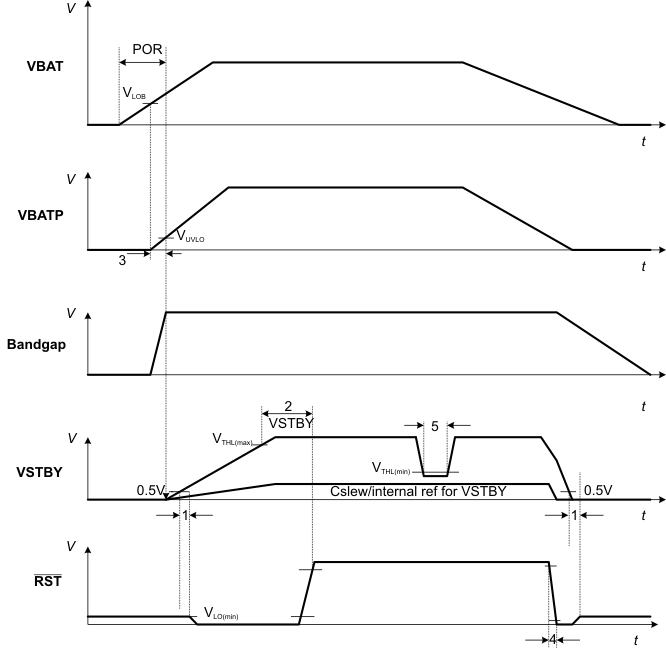 Figure 1. Input and Control Timing
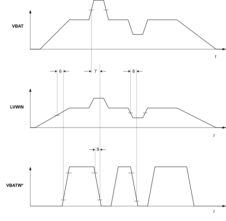 Figure 2. Input and Control Timing for VBATW
 Figure 3. Serial Communication AC Timing (I2C Interface)
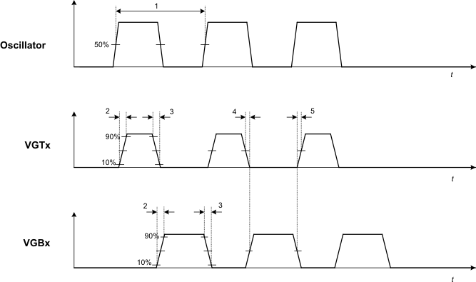 Figure 4. Switching Regulators Timing
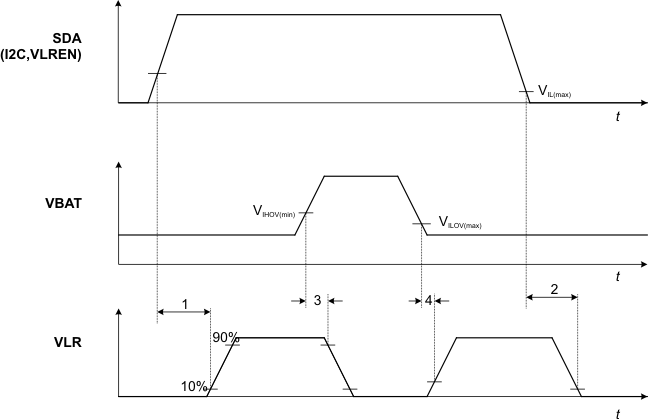 Figure 5. Linear Regulator Timing
 Figure 6. HSD Timing
6.17 Typical Characteristics
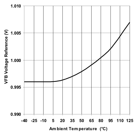 Figure 7. Feedback Reference vs Ambient Temperature
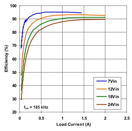 Figure 9. Efficiency vs Load Current
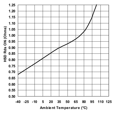 Figure 11. HSD RDS ON Resistance vs Ambient Temperature
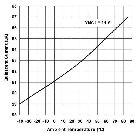 Figure 13. Quiescent Current vs Ambient Temperature
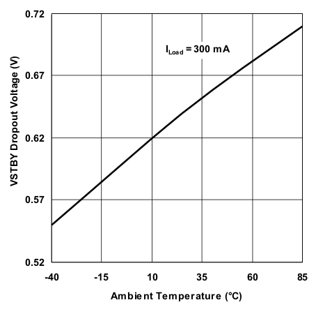 Figure 15. VSTBY Dropout Voltage vs Ambient Temperature
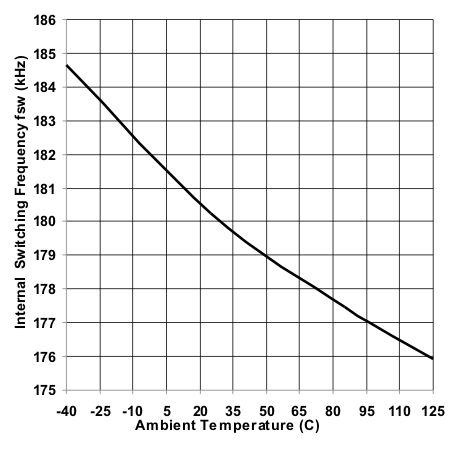 Figure 8. Internal Fixed Switching Frequency vs Ambient Temperature
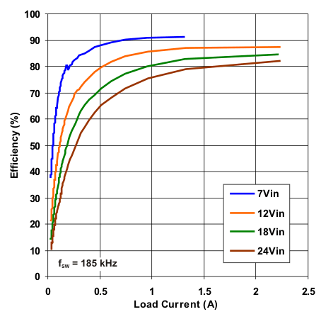 Figure 10. Efficiency vs Load Current
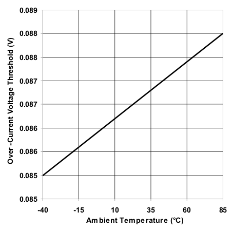 Figure 12. Overcurrent Voltage Threshold vs Ambient Temperature
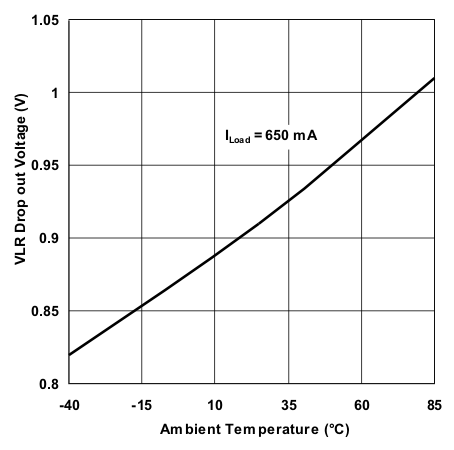 Figure 14. VLR Dropout Voltage vs Ambient Temperature