SLVSB16E November 2011 – December 2015 TPS43340-Q1
PRODUCTION DATA.
- 1 Features
- 2 Applications
- 3 Description
- 4 Revision History
- 5 Pin Configuration and Functions
- 6 Specifications
-
7 Detailed Description
- 7.1 Overview
- 7.2 Functional Block Diagram
- 7.3 Feature Description
- 7.4 Device Functional Modes
- 8 Application and Implementation
- 9 Power Supply Recommendations
- 10Layout
- 11Device and Documentation Support
- 12Mechanical, Packaging, and Orderable Information
Package Options
Mechanical Data (Package|Pins)
- PHP|48
Thermal pad, mechanical data (Package|Pins)
- PHP|48
Orderable Information
6 Specifications
6.1 Absolute Maximum Ratings
over operating free-air temperature range (unless otherwise noted)(1)(1) Stresses beyond those listed under Absolute Maximum Ratings may cause permanent damage to the device. These are stress ratings only, which do not imply functional operation of the device at these or any other conditions beyond those indicated under Recommended Operating Conditions. Exposure to absolute-maximum-rated conditions for extended periods may affect device reliability.
6.2 ESD Ratings
| VALUE | UNIT | |||||
|---|---|---|---|---|---|---|
| V(ESD) | Electrostatic discharge | Human body model (HBM), per AEC Q100-002(1) | All pins except VLR1 | ±2000 | V | |
| VLR1 | ±1000 | |||||
| Charged device model (CDM), per AEC Q100-011 | Corner pins (1, 12, 13, 24, 25, 36, 37, and 48) | ±750 | ||||
| Other pins | ±500 | |||||
| Machine model (MM) | All pins except RSTx | ±200 | ||||
| RSTx | ±100 | |||||
(1) AEC Q100-002 indicates HBM stressing is done in accordance with the ANSI/ESDA/JEDEC JS-001 specification.
6.3 Recommended Operating Conditions
over operating free-air temperature range (unless otherwise noted)6.4 Thermal Information
| THERMAL METRIC(1) | TPS43340-Q1 | UNIT | |
|---|---|---|---|
| PHP (HTQFP) | |||
| 48 PINS | |||
| RθJA | Junction-to-ambient thermal resistance | 26.3 | °C/W |
| RθJC(top) | Junction-to-case (top) thermal resistance | 12.2 | °C/W |
| RθJB | Junction-to-board thermal resistance | 7.2 | °C/W |
| ψJT | Junction-to-top characterization parameter | 0.2 | °C/W |
| ψJB | Junction-to-board characterization parameter | 7.1 | °C/W |
| RθJC(bot) | Junction-to-case (bottom) thermal resistance | 0.5 | °C/W |
(1) For more information about traditional and new thermal metrics, see the Semiconductor and IC Package Thermal Metrics application report (SPRA953).
6.5 Electrical Characteristics
VIN = VLR1 = 8 V to 18 V, VSUP = 4 V to 10 V, VIN2SENSE = 4 V to 40 V, TJ = –40°C to 150°C (unless otherwise noted)| PARAMETER | TEST CONDITIONS | MIN | TYP | MAX | UNIT | ||
|---|---|---|---|---|---|---|---|
| INPUT SUPPLY | |||||||
| VIN | Input voltage required for device on initial start-up | 6.5 | 40 | V | |||
| Operating range after initial start-up | 4 | V | |||||
| VIN UV | Undervoltage lockout | VIN falling. After a reset, initial start-up conditions may apply.(1) | 3.5 | 3.6 | 3.8 | V | |
| VIN rising. After a reset, initial start-up conditions may apply.(1) | 3.8 | 4 | V | ||||
| VLR1 | Device operating range for linear regulator | 4 | 40 | V | |||
| IQ | Quiescent current | TA = 25°C | EN1 = 1, LPM; EN2,3,4 = 0 | 30 | 40 | µA | |
| EN2 = 1, LPM; EN1,3,4 = 0 | 30 | 40 | |||||
| EN4 = 1, LPM; EN1,2,3 = 0 | 48 | 60 | |||||
| EN1,2 = 1, LPM; EN3,4 = 0 | 35 | 45 | |||||
| EN3,4 = 1, EN1,2 = 0 | 4 | 4.5 | mA | ||||
| TA = 125°C | EN1 = 1, LPM; EN2,3,4 = 0 | 40 | 50 | µA | |||
| EN2 = 1, LPM; EN1,3,4 = 0 | 40 | 50 | |||||
| EN4 = 1, LPM; EN1,2,3 = 0 | 52 | 60 | |||||
| EN1,2 = 1, LPM; EN3,4 = 0 | 40 | 45 | |||||
| EN3,4 = 1, EN1,2 = 0 | 5 | mA | |||||
| IVIN | Quiescent current | TA = 25°C | VIN = 13 V, Buck1: CCM, Buck2: off, or VIN = 13 V, Buck2: CCM, Buck1: off, or VIN = 13 V, Buck1 and Buck2: CCM |
5 | mA | ||
| TA = 125°C | Normal operation, SYNC = 5 V | 5 | mA | ||||
| VIN = 13 V, Buck1: CCM, Buck2: off | 5 | ||||||
| VIN = 13 V, Buck2: CCM, Buck1: off | 5 | ||||||
| VIN = 13 V, Buck1, 2: CCM | 7 | ||||||
| IVIN-SD | Shutdown current at TA = 25°C | EN1,2,3,4 = 0: off, VIN = VLR1 = 13 V | 5 | 10 | µA | ||
| IVIN-SD | Shutdown current at TA = 125°C | EN1,2,3,4 = 0: off, VIN = VLR1 = 13 V | 20 | µA | |||
| IVLRI-SD | Shutdown current at TA = 125°C | EN1,2,3,4 = 0: off, VIN = VLR1 = 13 V | 5 | µA | |||
| INTERNAL SUPPLY VREG | |||||||
| VREG | Internal regulated supply | VIN = 8 V to 18 V, EXTSUP = 0 V, SYNC = High | 5.5. | 5.8 | 6.1 | V | |
| Load regulation | EXTSUP = 0 V, SYNC = High IVREG = 0 mA to 100 mA | 0.2% | 1% | ||||
| VREG-EXTSUP | Internal regulated supply | EXTSUP = 8.5 V | 7.2. | 7.5 | 7.8 | V | |
| Load regulation | EXTSUP = 8.5 V to 13 V, IVREG = 0 mA to 125 mA, SYNC = High | 0.2% | 1% | ||||
| VEXTSUP-VREG | EXTSUP switch-over voltage | IVREG = 0 mA to 100 mA, EXTSUP ramping positive | 4.4 | 4.6 | 4.8 | V | |
| VEXTSUP-HYS | EXTSUP switch-over hysteresis | 150 | 250 | mV | |||
| IREG-LIM | Current limit on VREG | EXTSUP = 0 V normal mode as well as LPM | 100 | 400 | mA | ||
| IREG-EXTSUP-LIM | Current limit on VREG when using EXTSUP | IVREG = 0 mA to 100 mA, EXTSUP = 8.5 V, SYNC = High | 125 | 400 | mA | ||
| INPUT VOLTAGE VIN - OVERVOLTAGE LOCK OUT AND REVERSE POLARITY PROTECTION | |||||||
| VOVLO | Overvoltage shutdown | VIN rising | 45 | 46 | 47 | V | |
| VIN falling | 43 | 44 | 45 | V | |||
| OVLOHys | Hysteresis | 1 | 2 | 3 | V | ||
| OVLOfilter | Filter time | 5 | µs | ||||
| VGD | Clamping voltage of ext. FET | VIN - GPULL | 17 | V | |||
| RGPULL | Internal resistance to GND | 500 | kΩ | ||||
| BUCK CONTROLLERS | |||||||
| VOUT1, VOUT2 | Adjustable output voltage range | 0.9 | 11 | V | |||
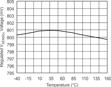
| VREF | Internal reference voltage and tolerance in normal mode | Measure VSENSEx pin | 0.792 | 0.8 | 0.808 | V | |
| –1% | 1% | ||||||
| VREF, LPM | Internal reference voltage and tolerance in low-power mode | Measure VSENSEx pin | 0.784 | 0.8 | 0.816 | V | |
| –2% | 2% | ||||||
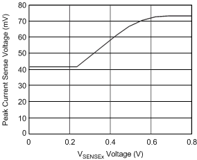
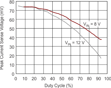
| VSENSE | VSENSE for forward-current limit in CCM | VSENSEx = 0.75 V, duty cycles < 10% | 60 | 75 | 90 | mV | |
| VSENSE for reverse-current limit in CCM | VSENSEx = 1 V | –65 | –37.5 | –23 | mV | ||
| VI-Foldback | VSENSE for output short | VSENSEx = 0 V (foldback) | 17 | 43.8 | 48 | mV | |
| tdead | Shoot through delay, blanking time | 20 | ns | ||||
| DCNRM | High-side minimum on-time | 100 | ns | ||||
| Maximum duty cycle (digitally controlled) | 98.75% | ||||||
| DCLPM | Duty cycle LPM | 80% | |||||
| ILPM_Entry | LPM entry threshold load current as fraction of maximum set load current | 1% | |||||
| VLPM_Exit | LPM exit threshold load current as fraction of maximum set load current | 10% | |||||
| HIGH-SIDE EXTERNAL NMOS GATE DRIVERS FOR BUCK CONTROLLERS | |||||||
| IGUx_peak | Gate driver peak current | 0.6 | A | ||||
| rDS(on) | Source and sink driver | VREG = 5.8 V, IGUx current = 200 mA | 5 | Ω | |||
| LOW-SIDE NMOS GATE DRIVERS FOR BUCK CONTROLLERS | |||||||
| IGLx_peak | Gate driver peak current | 0.6 | A | ||||
| rDS(on) | Source and sink driver | VREG = 5.8V, IGLx current = 200 mA | 5 | Ω | |||
| INTERNAL OSCILLATOR (RT) | |||||||
| fSW | Buck switching frequency | RT pin: GND | 360 | 400 | 440 | kHz | |
| fSW | Buck switching frequency | RT pin: 60 kΩ external resistor | 360 | 400 | 440 | kHz | |
| fSW-adj | Buck adjustable range with external resistor | RT pin: external resistor | 150 | 600 | kHz | ||
| fsync | Buck synch. range | External clock input on SYNC | 150 | 600 | kHz | ||
| VRT | Oscillator reference voltage | 1.2 | V | ||||
| tSW-Prop dly | SYNC rising edge to PH rising edge delay | 0 | 20 | 40 | ns | ||
| tSW-Trans-delay | Last SYNC rising edge to return to resistor mode if CLK is not present on SYNC pin | 20 | µs | ||||
| ERROR AMPLIFIER (OTA) FOR BUCK CONTROLLERS AND BUCK CONVERTER | |||||||
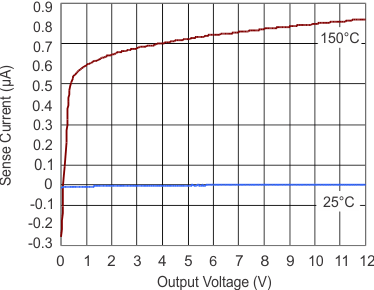
| IPULLUP_VSENSEx | Pullup current at VSENSEx pins | VSENSEx = 0 V | 50 | 100 | 200 | nA | |
| gm | Forward transconductance | COMP1, COMP2 = 0.8 V; source/sink = 5 µA, Test in feedback loop | 0.7 | 0.9 | 1.35 | mS | |
| EXTERNAL CLOCK AND ENABLE INPUTS: SYNC. EN1, EN2, EN3, EN4 | |||||||
| VIH | Higher threshold | VIN = 13 V | 1.7 | V | |||
| VIL | Lower threshold | VIN = 13 V | 0.7 | V | |||
| RIH | Pulldown resistance | VSYNC = 5 V | 500 | kΩ | |||
| IIL_ENx | Pullup current | VENx = 0V | 0.5 | 2 | µA | ||
| tdeglitch | Deglitch time, ENx | 2 | 16 | µs | |||
| LINEAR REGULATOR LREG1 | |||||||
| VLREG1 | Regulated output range | IL = 10 µA to 300 mA | 0.8 | 5.25 | V | ||
| VREF | Internal reference voltage tolerance | Referred to 0.8-V VREF, measured at VSENSE4 | –2.5% | 2.5% | |||
| Vline-reg | Line regulation | VIN = VLR1: 6 V to 28 V, IOUT 4 = 10 mA, | ∆VOUT, VOUT = 5 V | 15 | mV | ||
| ∆VOUT, VOUT = 3.3 V | 15 | ||||||
| ∆VOUT, VOUT = 1.5 V | 15 | ||||||
| Vload-reg | Load regulation | IOUT4 = 10 mA to 300 mA, VIN = 14 V | ∆VOUT, VOUT = 5 V | 10 | mV | ||
| ∆VOUT, VOUT = 3.3 V | 10 | ||||||
| ∆VOUT, VOUT = 1.5 V | 10 | ||||||
| VDropout | Drop out voltage | VIN = VLR1 = 4 V: IOUT = 250 mA | 500 | mV | |||
| VIN = 9 V, VLR1 = 4 V: IOUT = 150 mA | 300 | ||||||
| IOUT4 | Output current | VOUT in regulation | 0.01 | 300 | mA | ||
| ILREG1-CL | Output current limit | VOUT = 0 V | 400 | 1000 | mA | ||
| dVLREG1 / dt | Output soft start slew rate | 5 | V/ms | ||||
| PSRR | Power supply ripple rejection | Vripple = 0.5 VPP, IOUT = 300 mA | Freq = 100 Hz | 60 | dB | ||
| Freq = 150 kHz | 25 | ||||||
| VTH-CP ONp | Charge-pump turnoff voltage, VIN rising | 9.4 | V | ||||
| Hysteresis | 0.18 | V | |||||
| ITH-CP-OFF | Low-load current-detection threshold | IOUT4 falling | 2 | mA | |||
| Low-load current-detection hysteresis | 4 | mA | |||||
| SOFT START SSX | |||||||
| ISSx | Soft-start source current | SSx = 0 V | 0.75 | 1 | 1.25 | µA | |
| RESET RSTx | |||||||
| RSTpullup | RST1 to S2, RST2 to S4, RST4 to LREG1 internal pullups | 50 | kΩ | ||||
| RSTxth1 | Reset threshold | VSENSEx falling | –5 | –7 | –9.5 | %VREF | |
| RSTxhys | Hysteresis | 2 | %VREF | ||||
| RSTxdrop | Voltage drop | IRSTx = 5 mA | 450 | mV | |||
| IRSTx = 1 mA | 100 | mV | |||||
| RSTxleak | Leakage | VS2 = VS4 = VRSTx = 13 V, RST4 = 8 V | 1 | µA | |||
| tdeglitch | Power-good deglitch time | 2 | 16 | µs | |||
| tdelay | Reset release delay | External capacitor = 1 nF | 1 | ms | |||
| tdelay_fix | Fixed reset delay | No external capacitor, Rdelay pin open | 20 | 50 | µs | ||
| IOH | Activate current source (current to charge external capacitor) | Current to charge external capacitor | 30 | 40 | 50 | µA | |
| IIL | Activate current sink (current to discharge external capacitor) | Current to discharge external capacitor | 30 | 40 | 50 | µA | |
| SYNCHRONOUS BUCK CONVERTER BUCK3 | |||||||
| VSUP | Buck3 supply voltage | 4 | 10 | V | |||
| VSUP_UV | Buck3 undervoltage lockout | VSUP falling | 3.6 | 3.7 | 3.8 | V | |
| VSUP rising | 3.7 | 3.8 | 3.9 | V | |||
| rDS(on) | High-side switch | VSUP = 9 V, VBoot3 –PH3 = 5.8 V | 0.14 | 0.28 | Ω | ||
| Low-side switch | VSUP = 9 V, VVREG-PGND3 = 5.8 V | 0.15 | 0.28 | Ω | |||
| IHS-Limit | High-side switch | 2.5 | A | ||||
| ILS-Limit | Low-side switch, current into PH3 | 2.38 | A | ||||
| VSUPLkg | VSUP leakage current | VSUP = 10 V for high side, EN3 = Low. TJ = 100°C | 1 | µA | |||
| IFB3 | Current foldback | VSENSE3 = 0 V | 1.9 | A | |||
| fSW-adj | Buck3 switching frequency range with external resistor | Using external resistor on RT/CLK | 150 | 600 | kHz | ||
| VSense | Feedback voltage | Internal ref = 0.8 V | –1.5% | 1.5% | |||
| fSW-f-back | 2-times - frequency foldback exit threshold, VSENSE3 rising | 0.65 | V | ||||
| 2-times - frequency foldback entry threshold, VSENSE3 falling | 0.6 | V | |||||
| Gm3 | Current loop transconductance | ΔIpeakPH3 / ΔVCOMP3 | 5.4 | S | |||
| DC3 | Minimum duty cycle | fSW = 400 kHz, SLEW = LOW or OPEN | 10% | ||||
| Maximum duty cycle | In dropout operation | 98.75% | |||||
| TOT-BUCK3 | Overtemperature sensor threshold, leads to Buck3 FET deactivation | 170 | °C | ||||
| TOT-BUCK3-HYS | Overtemperature sensor hysteresis | 15 | °C | ||||
| THERMAL SHUTDOWN | |||||||
| Tshutdown | Junction temperature shutdown threshold | 150 | 170 | °C | |||
| Thys | Junction temperature hysteresis | 15 | °C | ||||
(1) If VBAT and VREG remain adequate, the buck can continue to operate if VIN is > 3.8 V
6.6 Typical Characteristics
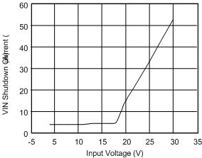
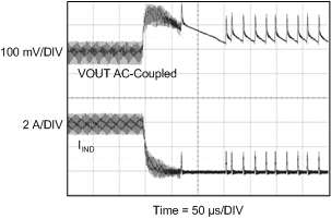
| VIN = 12 V | VOUTx = 5 V | RSENSE = 10 mΩ |
| Inductor = 4.7 µH | Switching Frequency = 400 kHz | |
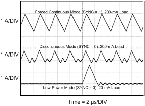
| VIN = 12 V | VOUTx = 5 V | RSENSE = 10 mΩ |
| Inductor = 4.7 µH | Switching Frequency = 400 kHz | |
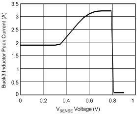
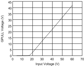
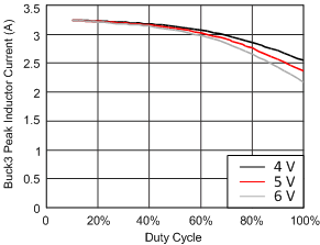
| VSUP = 4, 5, OR 6 V | Inductor = 10 µH | VSENSE3 = 0.75 V | ||
| Switching Frequency = 400 kHz | ||||
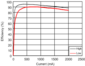
| VIN = 14 V | VOUT = 3.3 V | VSUP = 4 V |
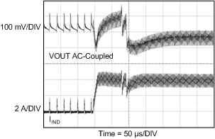
| VIN = 12 V | VOUTx = 5 V | RSENSE = 10 mΩ |
| Inductor = 4.7 µH | Switching Frequency = 400 kHz | |
