SLUSDX7A September 2020 – October 2020 TPS51397A
PRODUCTION DATA
- 1 Features
- 2 Applications
- 3 Description
- 4 Revision History
- 5 Pin Configuration and Functions
- 6 Specifications
- 7 Detailed Description
- 8 Application and Implementation
- 9 Power Supply Recommendations
- 10Layout
- 11Device and Documentation Support
- 12Mechanical, Packaging, and Orderable Information
Package Options
Mechanical Data (Package|Pins)
- RJE|20
Thermal pad, mechanical data (Package|Pins)
- RJE|20
Orderable Information
8.2.3 Application Curves
Figure 8-2 through Figure 8-17 apply to the circuit of Figure 8-1. VIN = 12 V, TA = 25°C, unless otherwise specified.
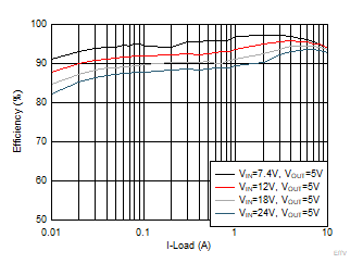 Figure 8-2 Efficiency Curve
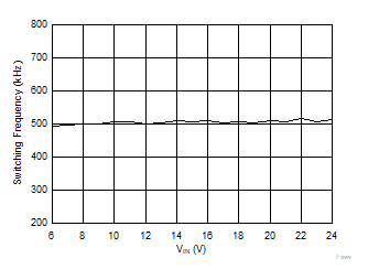 Figure 8-4 Switching Frequency vs
Input Voltage, IOUT = 5 A
 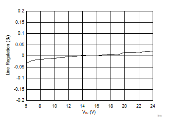 Figure 8-6 Line Regulation,
IOUT = 0.1 A
 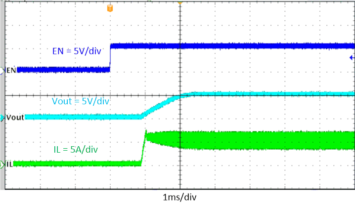 Figure 8-8 Start-Up Through EN,
IOUT = 5 A
 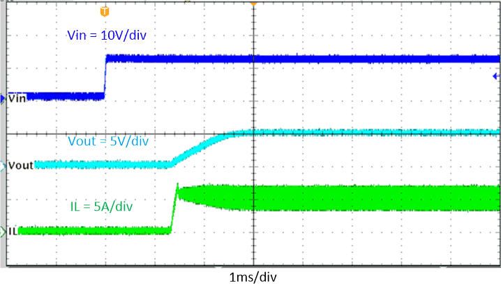 Figure 8-10 Start-up Relative to VIN
Rising,
 IOUT = 5 A
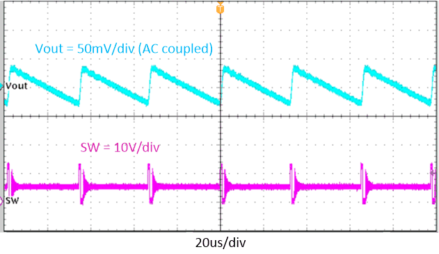 Figure 8-12 Output Voltage Ripple,
IOUT = 0.1 A
 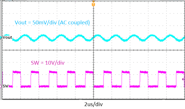 Figure 8-14 Output Voltage Ripple,
IOUT = 10 A
 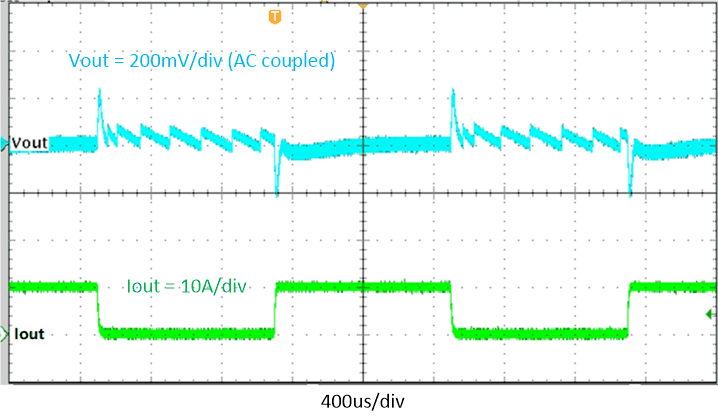 Figure 8-16 Transient Response, 0 A to
10 A,
 Slew Rate = 2.5 A/μs
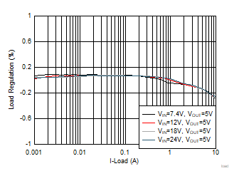 Figure 8-3 Load Regulation
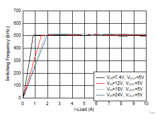 Figure 8-5 Switching Frequency vs
Output Load
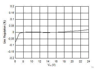 Figure 8-7 Line Regulation,
IOUT = 5 A
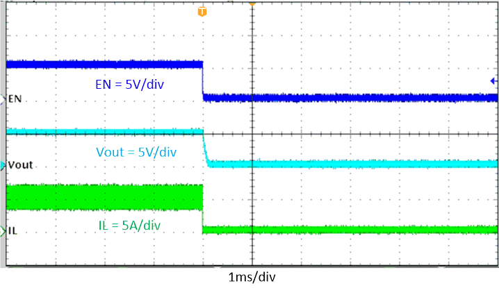 Figure 8-9 Shut-down Through EN,
IOUT = 5 A
 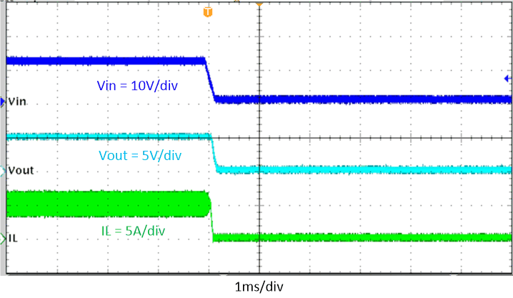 Figure 8-11 Shut Down Relative to VIN
Falling,
 IOUT = 5 A
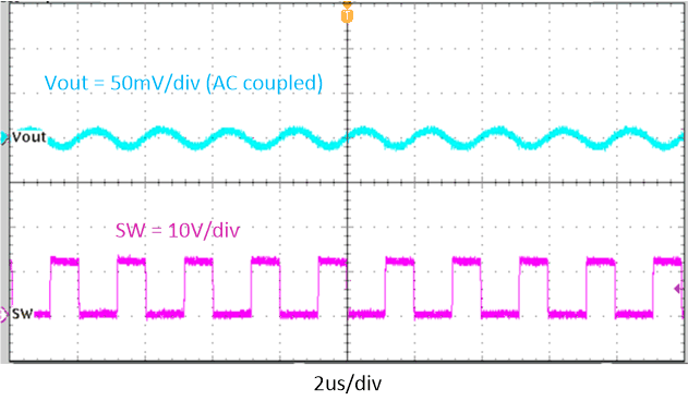 Figure 8-13 Output Voltage Ripple,
IOUT = 5 A
 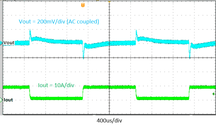 Figure 8-15 Transient Response, 1 A to
9 A,
 Slew Rate = 2.5 A/μs
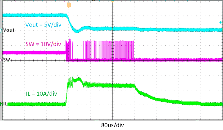 Figure 8-17 Normal Operation to Output
Hard Short