SLVSAV1D May 2011 – July 2016 TPS54062
PRODUCTION DATA.
- 1 Features
- 2 Applications
- 3 Description
- 4 Revision History
- 5 Pin Configuration and Functions
- 6 Specifications
-
7 Detailed Description
- 7.1 Overview
- 7.2 Functional Block Diagram
- 7.3
Feature Description
- 7.3.1 Fixed-Frequency PWM Control
- 7.3.2 Slope Compensation Output Current
- 7.3.3 Error Amplifier
- 7.3.4 Voltage Reference
- 7.3.5 Adjusting the Output Voltage
- 7.3.6 Enable and Adjusting Undervoltage Lockout
- 7.3.7 Constant Switching Frequency and Timing Resistor (RT/CLK Pin)
- 7.3.8 Selecting the Switching Frequency
- 7.3.9 How to Interface to RT/CLK Pin
- 7.3.10 Overvoltage Transient Protection
- 7.3.11 Thermal Shutdown
- 7.4 Device Functional Modes
-
8 Applications and Implementation
- 8.1 Application Information
- 8.2
Typical Applications
- 8.2.1
Continuous Conduction Mode (CCM) Switching Regulator
- 8.2.1.1 Design Requirements
- 8.2.1.2
Detailed Design Procedure
- 8.2.1.2.1 Selecting the Switching Frequency
- 8.2.1.2.2 Output Inductor Selection (LO)
- 8.2.1.2.3 Output Capacitor
- 8.2.1.2.4 Input capacitor
- 8.2.1.2.5 Bootstrap Capacitor Selection
- 8.2.1.2.6 Under Voltage Lock Out Set Point
- 8.2.1.2.7 Output Voltage and Feedback Resistors Selection
- 8.2.1.2.8 Closing the Loop
- 8.2.1.3 Application Curves
- 8.2.2 DCM Application
- 8.2.1
Continuous Conduction Mode (CCM) Switching Regulator
- 9 Power Supply Recommendations
- 10Layout
- 11Device and Documentation Support
- 12Mechanical, Packaging, and Orderable Information
Package Options
Mechanical Data (Package|Pins)
Thermal pad, mechanical data (Package|Pins)
- DRB|8
Orderable Information
6 Specifications
6.1 Absolute Maximum Ratings(1)
over operating free-air temperature range (unless otherwise noted)(1) The Absolute Maximum Ratings specified in this section will apply to all specifications of this document unless otherwise noted. These specifications will be interpreted as the conditions which may damage the device with a single occurrence.
6.2 ESD Ratings
| VALUE | UNIT | |||
|---|---|---|---|---|
| V(ESD) | Electrostatic discharge | Human-body model (HBM), per ANSI/ESDA/JEDEC JS-001(1) | ±2000 | V |
| Charged-device model (CDM), per JEDEC specification JESD22-C101(2) | ±500 | |||
(1) JEDEC document JEP155 states that 500-V HBM allows safe manufacturing with a standard ESD control process.
(2) JEDEC document JEP157 states that 250-V CDM allows safe manufacturing with a standard ESD control process.
6.3 Recommended Operating Conditions
over operating free-air temperature range (unless otherwise noted)| MIN | MAX | UNIT | ||
|---|---|---|---|---|
| Input coltage | 4.7 | 60 | V | |
| Output current | 50 | mA | ||
| Switching frequency set by RT/CLK resistor | 100 | 400 | kHz | |
| Switching frequency synchronized to external clock | 300 | 400 | kHz | |
6.4 Thermal Information
| THERMAL METRIC(1) | TPS54062 | UNIT | ||
|---|---|---|---|---|
| MSOP | VSON | |||
| 8 PINS | 8 PINS | |||
| RθJA | Junction-to-ambient thermal resistance | 127.1 | 40.2 | °C/W |
| RθJC(top) | Junction-to-case (top) thermal resistance | 33.4 | 49.7 | |
| RθJB | Junction-to-board thermal resistance | 80 | 15.7 | |
| ψJT | Junction-to-top characterization parameter | 1 | 0.6 | |
| ψJB | Junction-to-board characterization parameter | 79 | 15.9 | |
| RθJC(bot) | Junction-to-case (bottom) thermal resistance | N/A | 4.1 | |
(1) For more information about traditional and new thermal metrics, see the Semiconductor and IC Package Thermal Metrics application report.
6.5 Electrical Characteristics(1)
TJ = –40°C to 125°C, VIN = 4.7 to 60 V (unless otherwise noted)(1) The Electrical Ratings specified in this section will apply to all specifications in this document unless otherwise noted. These specifications will be interpreted as conditions that will not degrade the device’s parametric or functional specifications for the life of the product containing it.
6.6 Typical Characteristics
 Figure 1. High-Side RDS(on) vs Temperature
 Figure 3. VREF Voltage vs Temperature
 Figure 5. Frequency vs Temperature
 Figure 7. Error Amp Transconductance vs Temperature
 Figure 9. Enable Pin Hysteresis Current
vs Temperature
 Figure 11. Enable Pin Pullup Current vs Input Voltage
 Figure 13. Supply Current (VIN pin) vs Input Voltage
 Figure 15. Supply Current (VIN pin) vs
Input Voltage (0V to VSTART) EN Pin Open
 Figure 17. Current Limit vs
Input Voltage
 Figure 2. Low-Side RDS(on) vs Temperature
 Figure 4. Frequency vs VSENSE Voltage
 Figure 6. Frequency vs RT/CLK Resistance
 Figure 8. Enable Pin Voltage vs Temperature
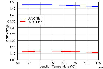
 Figure 10. Input Voltage (UVLO) vs Temperature
 Figure 12. Shutdown Supply Current (VIN) vs Input Voltage
 Figure 14. Supply Current (VIN pin)
 vs Input Voltage (0V to VSTART) EN Pin Low
 Figure 16. Slow-Start Time vs Temperature