SLVS500D DECEMBER   2003  – June 2019 TPS54110

PRODUCTION DATA.  

  1. Features
  2. Applications
  3. Description
    1.     Device Images
  4. Revision History
  5. Device Information
  6. Pin Configuration and Functions
    1.     Pin Functions
  7. Specifications
    1. 7.1 Absolute Maximum Ratings
    2. 7.2 Recommended Operating Conditions
    3. 7.3 Thermal Information
    4. 7.4 Electrical Characteristics
    5. 7.5 Typical Characteristics
  8. Detailed Description
    1. 8.1 Overview
    2. 8.2 Functional Block Diagram
    3. 8.3 Feature Description
      1. 8.3.1 VBIAS Regulator (VBIAS)
      2. 8.3.2 Voltage Reference
      3. 8.3.3 Oscillator and PWM Ramp
      4. 8.3.4 Error Amplifier
      5. 8.3.5 PWM Control
      6. 8.3.6 Dead-Time Control and MOSFET Drivers
      7. 8.3.7 Overcurrent Protection
      8. 8.3.8 Thermal Shutdown
      9. 8.3.9 Power Good (PWRDG)
    4. 8.4 Undervoltage Lockout (UVLO)
    5. 8.5 Slow-Start/Enable (SS/ENA)
  9. Application and Implementation
    1. 9.1 Application Information
    2. 9.2 Typical Applications
      1. 9.2.1 Typical TPS54110 Application
        1. 9.2.1.1 Design Requirements
        2. 9.2.1.2 Detailed Design Procedure
          1. 9.2.1.2.1 Switching Frequency
          2. 9.2.1.2.2 Input Capacitors
          3. 9.2.1.2.3 Output Filter Components
            1. 9.2.1.2.3.1 Inductor Selection
            2. 9.2.1.2.3.2 Capacitor Selection
          4. 9.2.1.2.4 Compensation Components
          5. 9.2.1.2.5 Bias and Bootstrap Capacitors
        3. 9.2.1.3 Application Curves
      2. 9.2.2 Very-Small Form-Factor Application
        1. 9.2.2.1 Design Requirements
        2. 9.2.2.2 Detailed Design Procedure
        3. 9.2.2.3 Application Curves
      3. 9.2.3 Two-Output Sequenced-Startup Application
        1. 9.2.3.1 Design Requirements
        2. 9.2.3.2 Detailed Design Procedure
        3. 9.2.3.3 Application Curve
  10. 10Layout
    1. 10.1 Layout Guidelines
    2. 10.2 Layout Example
    3. 10.3 Layout Considerations For Thermal Performance
    4. 10.4 Grounding and Powerpad Layout
  11. 11Device and Documentation Support
    1. 11.1 Device Support
      1. 11.1.1 Third-Party Products Disclaimer
    2. 11.2 Receiving Notification of Documentation Updates
    3. 11.3 Community Resources
    4. 11.4 Trademarks
    5. 11.5 Electrostatic Discharge Caution
    6. 11.6 Glossary
  12. 12Mechanical, Packaging, and Orderable Information

Package Options

Refer to the PDF data sheet for device specific package drawings

Mechanical Data (Package|Pins)
  • PWP|20
Thermal pad, mechanical data (Package|Pins)
Orderable Information

Application Curves

All performance data shown for VI = 5 V, VO = 3.3 V, fs = 700 kHz, TA = 25°C, Figure 9
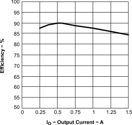
TPS54110 perform_fig11_lvs500.gif
Figure 10. Efficiency vs Output Current
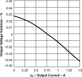
TPS54110 perform_fig13_lvs500.gif
Figure 12. Load Regulation vs Output Current
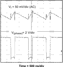
TPS54110 perform_fig15_lvs500.gif
Figure 14. Input Voltage Ripple
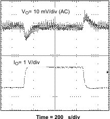
TPS54110 perform_fig17_lvs500.gif
Figure 16. Output Voltage Transient Response
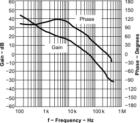
TPS54110 perform_fig19_lvs500.gif
Figure 18. Measured Loop Response
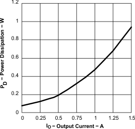
TPS54110 perform_fig12_lvs500.gif
Figure 11. Power Dissipation vs Output Current
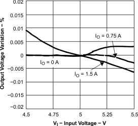
TPS54110 perform_fig14_lvs500.gif
Figure 13. Line Regulation vs Input Voltage
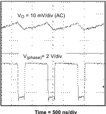
TPS54110 perform_fig16_lvs500.gif
Figure 15. Output Voltage Ripple
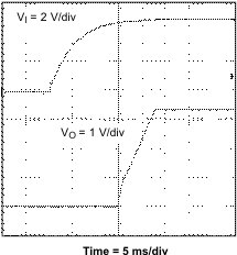
TPS54110 perform_fig18_lvs500.gif
Figure 17. Start Up Waveform