SLVS500D DECEMBER   2003  – June 2019 TPS54110

PRODUCTION DATA.  

  1. Features
  2. Applications
  3. Description
    1.     Device Images
  4. Revision History
  5. Device Information
  6. Pin Configuration and Functions
    1.     Pin Functions
  7. Specifications
    1. 7.1 Absolute Maximum Ratings
    2. 7.2 Recommended Operating Conditions
    3. 7.3 Thermal Information
    4. 7.4 Electrical Characteristics
    5. 7.5 Typical Characteristics
  8. Detailed Description
    1. 8.1 Overview
    2. 8.2 Functional Block Diagram
    3. 8.3 Feature Description
      1. 8.3.1 VBIAS Regulator (VBIAS)
      2. 8.3.2 Voltage Reference
      3. 8.3.3 Oscillator and PWM Ramp
      4. 8.3.4 Error Amplifier
      5. 8.3.5 PWM Control
      6. 8.3.6 Dead-Time Control and MOSFET Drivers
      7. 8.3.7 Overcurrent Protection
      8. 8.3.8 Thermal Shutdown
      9. 8.3.9 Power Good (PWRDG)
    4. 8.4 Undervoltage Lockout (UVLO)
    5. 8.5 Slow-Start/Enable (SS/ENA)
  9. Application and Implementation
    1. 9.1 Application Information
    2. 9.2 Typical Applications
      1. 9.2.1 Typical TPS54110 Application
        1. 9.2.1.1 Design Requirements
        2. 9.2.1.2 Detailed Design Procedure
          1. 9.2.1.2.1 Switching Frequency
          2. 9.2.1.2.2 Input Capacitors
          3. 9.2.1.2.3 Output Filter Components
            1. 9.2.1.2.3.1 Inductor Selection
            2. 9.2.1.2.3.2 Capacitor Selection
          4. 9.2.1.2.4 Compensation Components
          5. 9.2.1.2.5 Bias and Bootstrap Capacitors
        3. 9.2.1.3 Application Curves
      2. 9.2.2 Very-Small Form-Factor Application
        1. 9.2.2.1 Design Requirements
        2. 9.2.2.2 Detailed Design Procedure
        3. 9.2.2.3 Application Curves
      3. 9.2.3 Two-Output Sequenced-Startup Application
        1. 9.2.3.1 Design Requirements
        2. 9.2.3.2 Detailed Design Procedure
        3. 9.2.3.3 Application Curve
  10. 10Layout
    1. 10.1 Layout Guidelines
    2. 10.2 Layout Example
    3. 10.3 Layout Considerations For Thermal Performance
    4. 10.4 Grounding and Powerpad Layout
  11. 11Device and Documentation Support
    1. 11.1 Device Support
      1. 11.1.1 Third-Party Products Disclaimer
    2. 11.2 Receiving Notification of Documentation Updates
    3. 11.3 Community Resources
    4. 11.4 Trademarks
    5. 11.5 Electrostatic Discharge Caution
    6. 11.6 Glossary
  12. 12Mechanical, Packaging, and Orderable Information

Package Options

Refer to the PDF data sheet for device specific package drawings

Mechanical Data (Package|Pins)
  • PWP|20
Thermal pad, mechanical data (Package|Pins)
Orderable Information

Grounding and Powerpad Layout

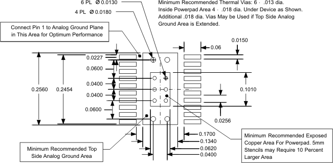
The TPS54110 has two internal grounds (analog and power). Inside the TPS54110, the analog ground connects all noise-sensitive signals, while the power ground connects the noisier power signals. The PowerPAD must be tied directly to AGND. Noise injected between the two grounds can degrade the performance of the TPS54110, particularly at higher output currents. However, ground noise on an analog ground plane can also cause problems with some of the control and bias signals. For these reasons, separate analog and power ground planes are recommended. Tie these two planes together directly at the IC to reduce noise between the two grounds. The only components that tie directly to the power-ground plane are the input capacitor, the output capacitor, the input voltage decoupling capacitor, and the PGND pins of the TPS54110. The layout of the TPS54110 evaluation module represents recommended layout for a 2-layer board. Documentation for the TPS54110 evaluation module is obtained from the Texas Instruments web site under the TPS54110 product folder and in the application note, TI literature number SLVA109.
TPS54110 land_pat_PowPad_lvs500.gifFigure 31. Recommended Land Pattern for 20-Pin PWP Powerpad