SLVS751E November 2007 – January 2024 TPS5430-Q1
PRODUCTION DATA
- 1
- 1 Features
- 2 Applications
- 3 Description
- 4 Pin Configuration and Functions
- 5 Specifications
-
6 Detailed Description
- 6.1 Overview
- 6.2 Functional Block Diagram
- 6.3
Feature Description
- 6.3.1 Oscillator Frequency
- 6.3.2 Voltage Reference
- 6.3.3 Enable (ENA) and Internal Slow Start
- 6.3.4 Undervoltage Lockout (UVLO)
- 6.3.5 Boost Capacitor (BOOT)
- 6.3.6 Output Feedback (VSENSE) and Internal Compensation
- 6.3.7 Voltage Feed Forward
- 6.3.8 Pulse-Width Modulation (PWM) Control
- 6.3.9 Overcurrent Limiting
- 6.3.10 Overvoltage Protection (OVP)
- 6.3.11 Thermal Shutdown
- 6.4 Device Functional Modes
-
7 Application and Implementation
- 7.1 Application Information
- 7.2
Typical Applications
- 7.2.1
Application Circuit, 12 V to 5 V
- 7.2.1.1 Design Requirements
- 7.2.1.2 Detailed Design Procedure
- 7.2.1.3 Application Curves
- 7.2.2 9-V to 21-V Input to 5-V Output Application Circuit
- 7.2.3 Circuit Using Ceramic Output Filter Capacitors
- 7.2.1
Application Circuit, 12 V to 5 V
- 7.3 Power Supply Recommendations
- 7.4 Layout
- 8 Device and Documentation Support
- 9 Revision History
- 10Mechanical, Packaging, and Orderable Information
Package Options
Mechanical Data (Package|Pins)
- DDA|8
Thermal pad, mechanical data (Package|Pins)
- DDA|8
Orderable Information
7.2.3.2 External Compensation Network
When using ceramic output capacitors, additional circuitry is required to stabilize the closed loop system. For this circuit, the external components are R3, C4, C6, and C7. To determine the value of these components, first calculate the LC resonant frequency of the output filter:
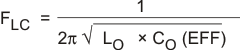
For this example, the effective resonant frequency is calculated as 4109 Hz.
The network composed of R1, R2, R3, C5, C6, and C7 has two poles and two zeros that are used to tailor the overall response of the feedback network to accommodate the use of the ceramic output capacitors. The pole and zero locations are given by the following equations:
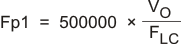


The final pole is located at a frequency too high to be of concern. The second zero, Fz2 as defined by Equation 26 uses 2.5 for the frequency multiplier. In some cases this can need to be slightly higher or lower. Values in the range of 2.3 to 2.7 work well. The values for R1 and R2 are fixed by the 3.3-V output voltage as calculated using Equation 12. For this design R1 = 10 kΩ and R2 = 5.90 kΩ. With Fp1 = 401 Hz, Fz1 = 2876 Hz, and Fz2 = 10.3 kHz, the values of R3, C6, and C7 are determined using Equation 27, Equation 28, and Equation 29:
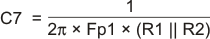
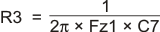
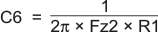
For this design, using the closest standard values, C7 is 0.1 μF, R3 is 549 Ω, and C6 is 1500 pF. C4 is added to improve load regulation performance. It is effectively in parallel with C6 in the location of the second pole frequency, so it must be small in relationship to C6. C4 must be less the 1/10 the value of C6. For this example, 150 pF works well.
For additional information on external compensation of the wide-voltage-range PWM converter devices, see Using TPS5410/20/30/31 With Aluminum/Ceramic Output Capacitors (SLVA237).