SLVSDG6B May 2016 – April 2021 TPS54302
PRODUCTION DATA
- 1 Features
- 2 Applications
- 3 Description
- 4 Revision History
- 5 Pin Configuration and Functions
- 6 Specifications
-
7 Detailed Description
- 7.1 Overview
- 7.2 Functional Block Diagram
- 7.3
Feature Description
- 7.3.1 Fixed-Frequency PWM Control
- 7.3.2 Pulse Skip Mode
- 7.3.3 Error Amplifier
- 7.3.4 Slope Compensation and Output Current
- 7.3.5 Enable and Adjusting Undervoltage Lockout
- 7.3.6 Safe Startup into Pre-Biased Outputs
- 7.3.7 Voltage Reference
- 7.3.8 Adjusting Output Voltage
- 7.3.9 Internal Soft-Start
- 7.3.10 Bootstrap Voltage (BOOT)
- 7.3.11 Overcurrent Protection
- 7.3.12 Spread Spectrum
- 7.3.13 Output Overvoltage Protection (OVP)
- 7.3.14 Thermal Shutdown
- 7.4 Device Functional Modes
- 8 Application and Implementation
- 9 Power Supply Recommendations
- 10Layout
- 11Device and Documentation Support
- 12Mechanical, Packaging, and Orderable Information
Package Options
Refer to the PDF data sheet for device specific package drawings
Mechanical Data (Package|Pins)
- DDC|6
Thermal pad, mechanical data (Package|Pins)
Orderable Information
7.3.11.2 Low-Side MOSFET Overcurrent Protection
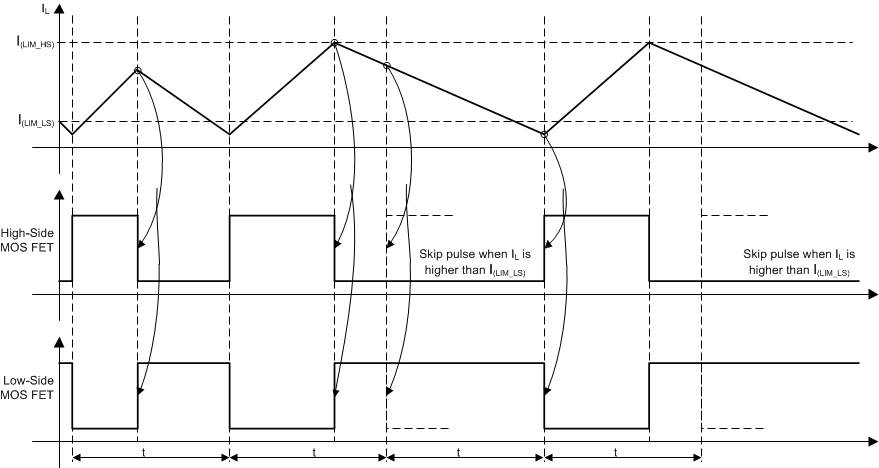
While the low-side MOSFET is turned on, the conduction current is monitored by the internal circuitry. During normal operation the low-side MOSFET sources current to the load. At the end of every clock cycle, the low-side MOSFET sourcing current is compared to the internally set low-side sourcing current-limit. The inductor valley current is exceeded the low-side source current limit, the high-side MOSFET does not turn on and the low-side MOSFET stays on for the next cycle. The high-side MOSFET turns on again when the inductor valley current is below the low-side sourcing current-limit at the start of a cycle as shown in Figure 7-2.

Furthermore, if an output overload condition occurs for more than the hiccup wait time, which is programmed for 512 switching cycles, the device shuts down and restarts after the hiccup time of 16384 cycles. The hiccup mode helps to reduce the device power dissipation under severe overcurrent conditions.