SLVSDV8 July 2017 TPS54424
PRODUCTION DATA.
- 1 Features
- 2 Applications
- 3 Description
- 4 Revision History
- 5 Pin Configuration and Functions
- 6 Specifications
-
7 Detailed Description
- 7.1 Overview
- 7.2 Functional Block Diagram
- 7.3
Feature Description
- 7.3.1 Fixed Frequency PWM Control
- 7.3.2 Continuous Conduction Mode Operation (CCM)
- 7.3.3 VIN Pins and VIN UVLO
- 7.3.4 Voltage Reference and Adjusting the Output Voltage
- 7.3.5 Error Amplifier
- 7.3.6 Enable and Adjustable UVLO
- 7.3.7 Soft Start and Tracking
- 7.3.8 Safe Start-up into Pre-Biased Outputs
- 7.3.9 Power Good
- 7.3.10 Sequencing (SS/TRK)
- 7.3.11 Adjustable Switching Frequency (RT Mode)
- 7.3.12 Synchronization (CLK Mode)
- 7.3.13 Bootstrap Voltage and 100% Duty Cycle Operation (BOOT)
- 7.3.14 Output Overvoltage Protection (OVP)
- 7.3.15 Overcurrent Protection
- 7.4 Device Functional Modes
-
8 Application and Implementation
- 8.1 Application Information
- 8.2
Typical Application
- 8.2.1 Design Requirements
- 8.2.2
Detailed Design Procedure
- 8.2.2.1 Custom Design With WEBENCH® Tools
- 8.2.2.2 Switching Frequency
- 8.2.2.3 Output Inductor Selection
- 8.2.2.4 Output Capacitor
- 8.2.2.5 Input Capacitor
- 8.2.2.6 Output Voltage Resistors Selection
- 8.2.2.7 Soft-start Capacitor Selection
- 8.2.2.8 Undervoltage Lockout Set Point
- 8.2.2.9 Bootstrap Capacitor Selection
- 8.2.2.10 PGOOD Pull-up Resistor
- 8.2.2.11 Compensation
- 8.2.3 Application Curves
- 9 Power Supply Recommendations
- 10Layout
- 11Device and Documentation Support
- 12Mechanical, Packaging, and Orderable Information
Package Options
Refer to the PDF data sheet for device specific package drawings
Mechanical Data (Package|Pins)
- RNV|18
Thermal pad, mechanical data (Package|Pins)
Orderable Information
8.2.3 Application Curves

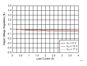
| TA = 25°C | VOUT = 1.8 V | fSW = 700 kHz |

| TA = 25°C | VOUT = 1.8 V | fSW = 700 kHz |

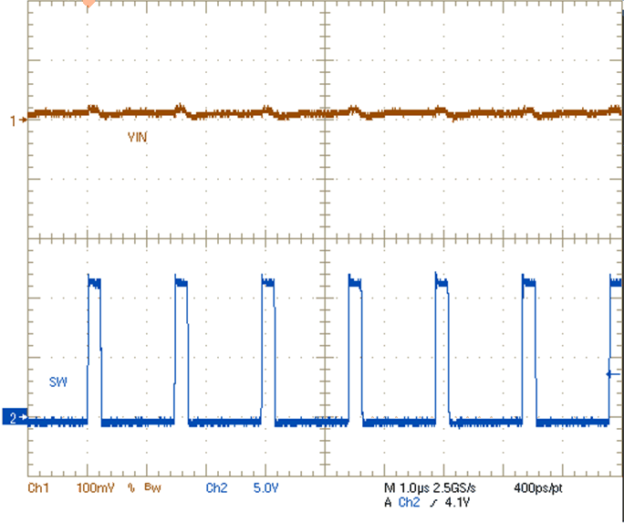
| VIN = 12 V | VOUT = 1.8 V | IOUT = 2 A |

| VIN = 12 V | VOUT = 1.8 V | IOUT = 0 A |

| VIN = 12 V | VOUT = 1.8 V | IOUT = 0 A |

| RLOAD = 1 Ω |

| RLOAD = 1 Ω | VIN = 12 V |

| VIN = 12 V |

| VIN = 12 V | IOUT = short |

| TA = 25°C | VOUT = 1.8 V | fSW = 700 kHz |

| TA = 25°C | VOUT = 1.8 V | fSW = 700 kHz |

| VIN = 12 V | VOUT = 1.8 V |

| VIN = 12 V | VOUT = 1.8 V | IOUT = 4 A |

| VIN = 12 V | VOUT = 1.8 V | IOUT = 4 A |

| RLOAD = 1 Ω |

| RLOAD = 1 Ω |

| VIN = 12 V | IOUT = short |

| VIN = 12 V | IOUT = short removed |