SLVSHC5B November 2023 – July 2024 TPS548D26
PRODUCTION DATA
- 1
- 1 Features
- 2 Applications
- 3 Description
- 4 Pin Configuration and Functions
- 5 Specifications
-
6 Detailed Description
- 6.1 Overview
- 6.2 Functional Block Diagram
- 6.3
Feature Description
- 6.3.1 Internal VCC LDO and Using an External Bias on the VCC and VDRV Pin
- 6.3.2 Input Undervoltage Lockout (UVLO)
- 6.3.3 Set the Output Voltage
- 6.3.4 Differential Remote Sense and Feedback Divider
- 6.3.5 Start-Up and Shutdown
- 6.3.6 Loop Compensation
- 6.3.7 Set Switching Frequency and Operation Mode
- 6.3.8 Switching Node (SW)
- 6.3.9 Overcurrent Limit and Low-side Current Sense
- 6.3.10 Negative Overcurrent Limit
- 6.3.11 Zero-Crossing Detection
- 6.3.12 Input Overvoltage Protection
- 6.3.13 Output Undervoltage and Overvoltage Protection
- 6.3.14 Overtemperature Protection
- 6.3.15 Power Good
- 6.4 Device Functional Modes
- 7 Application and Implementation
- 8 Device and Documentation Support
- 9 Revision History
- 10Mechanical, Packaging, and Orderable Information
Package Options
Mechanical Data (Package|Pins)
- RXX|37
Thermal pad, mechanical data (Package|Pins)
- RXX|37
Orderable Information
7.2.4 Application Curves

| PVIN = 12V |
VCC = Internal LDO |
VOUT = 1.1V |
|
MODE = FCCM |

| PVIN = 12V |
VCC = External 5V Bias |
VOUT = 1.1V |
|
MODE = FCCM |

| PVIN = 12V | VCC = External 5V Bias | VOUT = 1.1V |
| MODE = DCM |

| PVIN = 12V | VCC = Internal LDO | VOUT = 1.1V |
| MODE = FCCM | No DC Load Line (DCLL) |

| PVIN = 12V | VCC = Internal LDO | VOUT = 1.1V |
| MODE = DCM | No DC Load Line (DCLL) |
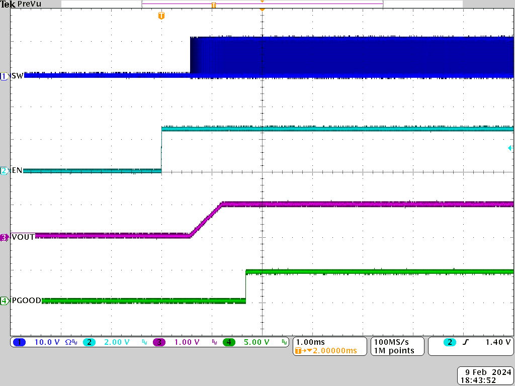 Figure 7-12 ENABLE Start-Up Waveform, PVIN = 12V,
VOUT = 1.1V
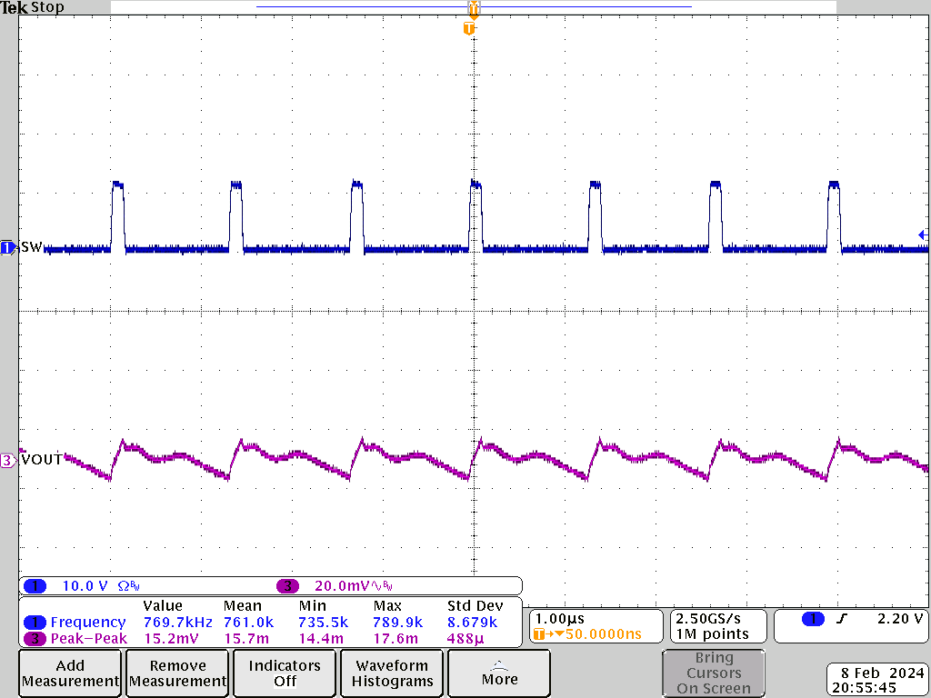 Figure 7-14 Output Voltage Ripple, 800kHz FCCM, 40A
Load, PVIN = 12V, VOUT = 1.1V
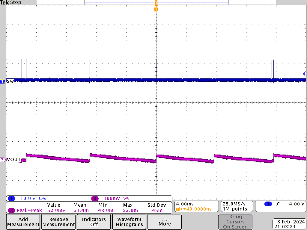 Figure 7-16 Output Voltage Ripple, DCM, No load, PVIN
= 12V, VOUT = 1.1V
| PVIN = 12V | VCC = Internal LDO | VOUT = 1.1V |
| MODE = FCCM |

| PVIN = 12V | VCC = External 5V Bias | VOUT = 1.1V |
| MODE = FCCM |

| PVIN = 12V | VCC = External 5V Bias | VOUT = 1.1V |
| MODE = DCM |

| PVIN = 12V |
VCC = External 5V Bias |
VOUT = 1.1V |
| MODE = FCCM | No DC Load Line (DCLL) |

| PVIN = 12V |
VCC = External 5V Bias |
VOUT = 1.1V |
| MODE = DCM | No DC Load Line (DCLL) |
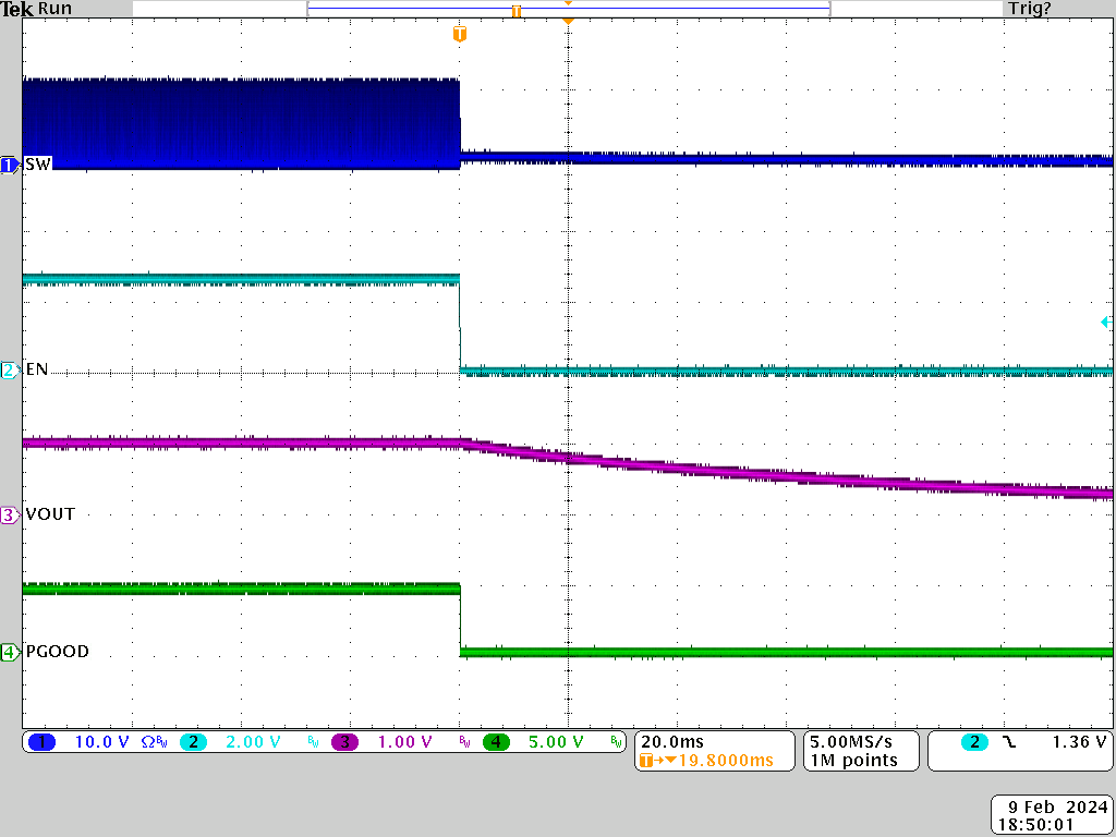 Figure 7-13 ENABLE Shutdown Waveform, PVIN = 12V,
VOUT = 1.1V
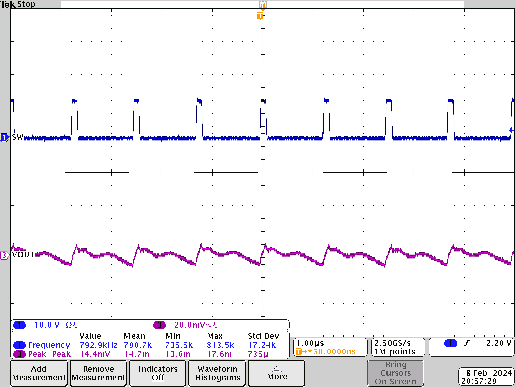 Figure 7-15 Output Voltage Ripple, 800kHz FCCM, No
load, PVIN = 12V, VOUT = 1.1V