SLVS847A November 2008 – December 2016 TPS54917
PRODUCTION DATA.
- 1 Features
- 2 Applications
- 3 Description
- 4 Revision History
- 5 Device Comparison Table
- 6 Pin Configuration and Functions
- 7 Specifications
-
8 Detailed Description
- 8.1 Overview
- 8.2 Functional Block Diagram
- 8.3
Feature Description
- 8.3.1 Undervoltage Lockout (UVLO)
- 8.3.2 Slow Start or Enable (SS/ENA)
- 8.3.3 VBIAS Regulator (VBIAS)
- 8.3.4 Voltage Reference
- 8.3.5 Oscillator and PWM Ramp
- 8.3.6 Error Amplifier
- 8.3.7 PWM Control
- 8.3.8 Dead-Time Control and MOSFET Drivers
- 8.3.9 Overcurrent Protection
- 8.3.10 Thermal Shutdown
- 8.3.11 Power Good (PWRGD)
- 8.4 Device Functional Modes
- 9 Application and Implementation
- 10Power Supply Recommendations
- 11Layout
- 12Device and Documentation Support
- 13Mechanical, Packaging, and Orderable Information
Package Options
Mechanical Data (Package|Pins)
- RUV|34
Thermal pad, mechanical data (Package|Pins)
- RUV|34
Orderable Information
1 Features
- 13-mΩ MOSFET Switches for High Efficiency at 9-A Continuous Output
- Adjustable Output Voltage Down to 0.9 V With
1% Accuracy - Externally Compensated for Design Flexibility
- Wide PWM Frequency: Fixed 350 kHz, 550 kHz, or Adjustable 280 kHz to 1.6 MHz
- Synchronizable to 1.6 MHz
- Load Protected by Peak Current Limit and Thermal Shutdown
- Small 3.5 mm x 7 mm Package and Similar Layout to TPS54910 Reduces Board Area and Total Cost
- SWIFT Documentation Application Notes, and SwitcherPro™ Software: www.ti.com/swift
2 Applications
- Low-Voltage, High-Density Systems With Power Distributed at 3.3 V
- Point-of-Load Regulation for High Performance DSPs, FPGAs, ASICs, and Microprocessors
- Broadband, Networking, and Optical Communications Infrastructure
3 Description
As a member of the SWIFT™ family of DC-DC regulators, the TPS54917 low-input voltage high-output current synchronous buck PWM converter offers the same features as the TPS54910 in a smaller package and higher switching frequency, which allows for a smaller total solution. Included on the substrate with the listed features are a true, high performance, voltage error amplifier that enables maximum performance under transient conditions and flexibility in choosing the output filter L and C components; an undervoltage lockout (UVLO) circuit to prevent start-up until the input voltage reaches 3 V; an internally and externally set slow-start circuit to limit in-rush currents; and a power good output useful for processor or logic reset, fault signaling, and supply sequencing.
The TPS54917 is available in a thermally enhanced 34-pin VQFN (RUV) PowerPAD™ package, which eliminates bulky heat sinks. TI provides evaluation modules and the SwitcherPro design software tool to aid in achieving high-performance power supply designs to meet aggressive equipment development cycles.
Device Information(1)
| PART NUMBER | PACKAGE | BODY SIZE (NOM) |
|---|---|---|
| TPS54917 | VQFN (34) | 3.50 mm × 7.00 mm |
- For all available packages, see the orderable addendum at the end of the data sheet.
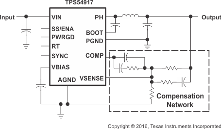
Simplified Schematic

Efficiency at 700 kHz
