SLUSDX0A September 2020 – August 2021 TPS562211
PRODUCTION DATA
- 1 Features
- 2 Applications
- 3 Description
- 4 Revision History
- 5 Pin Configuration and Functions
- 6 Specifications
-
7 Detailed Description
- 7.1 Overview
- 7.2 Functional Block Diagram
- 7.3
Feature Description
- 7.3.1 Advanced Emulated Current Mode Control
- 7.3.2 Mode Selection and PG/SS Pin Function Configuration
- 7.3.3 Power Good (PG)
- 7.3.4 Soft Start and Pre-Biased Soft Start
- 7.3.5 Output Discharge through PG/SS Pin
- 7.3.6 Precise Enable and Adjusting Undervoltage Lockout
- 7.3.7 Overcurrent Limit and Undervoltage Protection
- 7.3.8 Overvoltage Protection
- 7.3.9 Thermal Shutdown
- 7.4 Device Functional Modes
- 8 Application and Implementation
- 9 Power Supply Recommendations
- 10Layout
- 11Device and Documentation Support
- 12Mechanical, Packaging, and Orderable Information
Package Options
Mechanical Data (Package|Pins)
- DRL|8
Thermal pad, mechanical data (Package|Pins)
Orderable Information
8.2.3 Application Curves
VIN = 12 V, L1= 4.7 μH, COUT = 44 μF, TA = 25°C (unless otherwise noted)
 Figure 8-2 Efficiency
 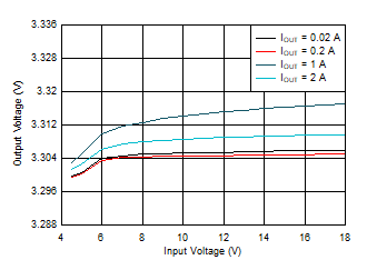 Figure 8-4 Line
Regulation
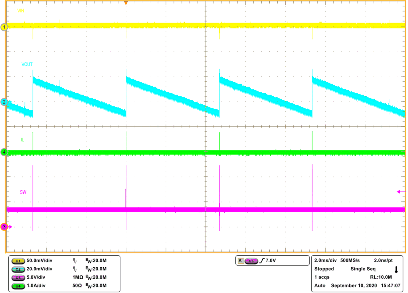 Figure 8-6 Steady State Waveforms, IOUT = 0 A
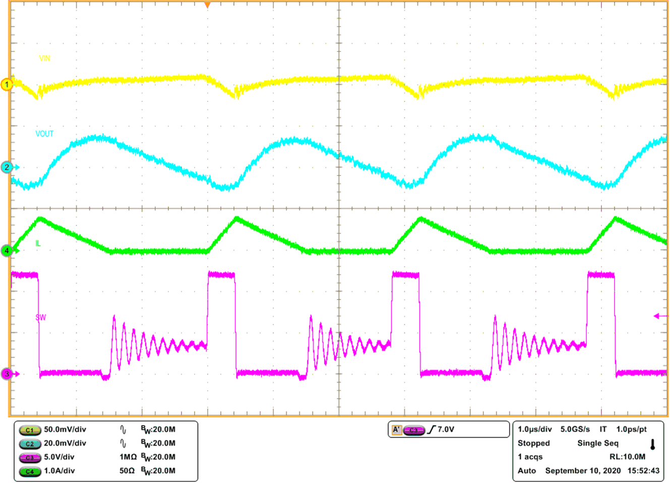 Figure 8-8 Steady State Waveforms, IOUT = 0.2 A
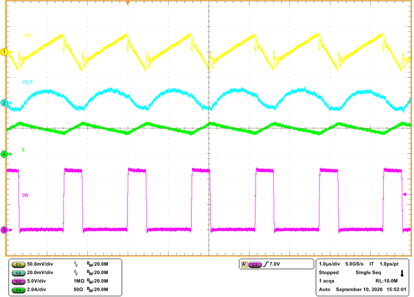 Figure 8-10 Steady State Waveforms, IOUT = 2 A
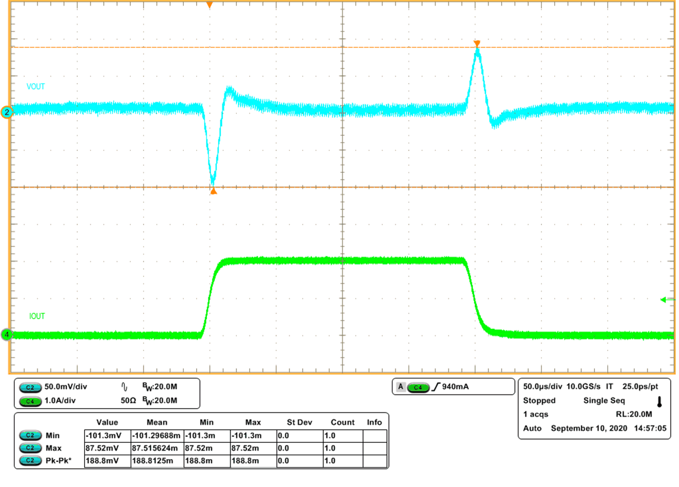 Figure 8-12 Transient Response 0 to 2 A with Slew Rate of 0.25 A/μs (FCCM)
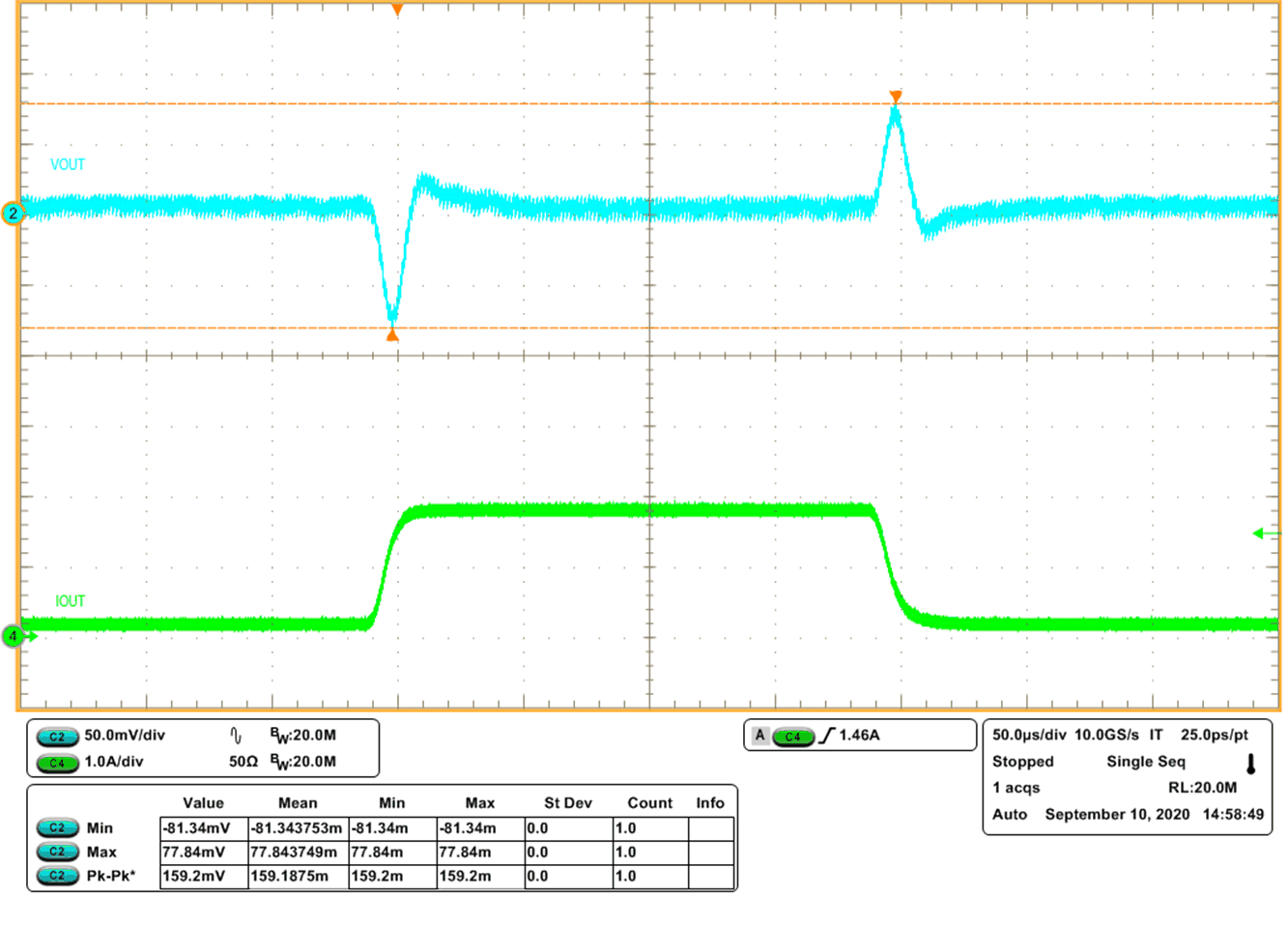 Figure 8-14 Transient Response 0.2 to 1.8 A with Slew Rate of 0.25 A/μs (FCCM)
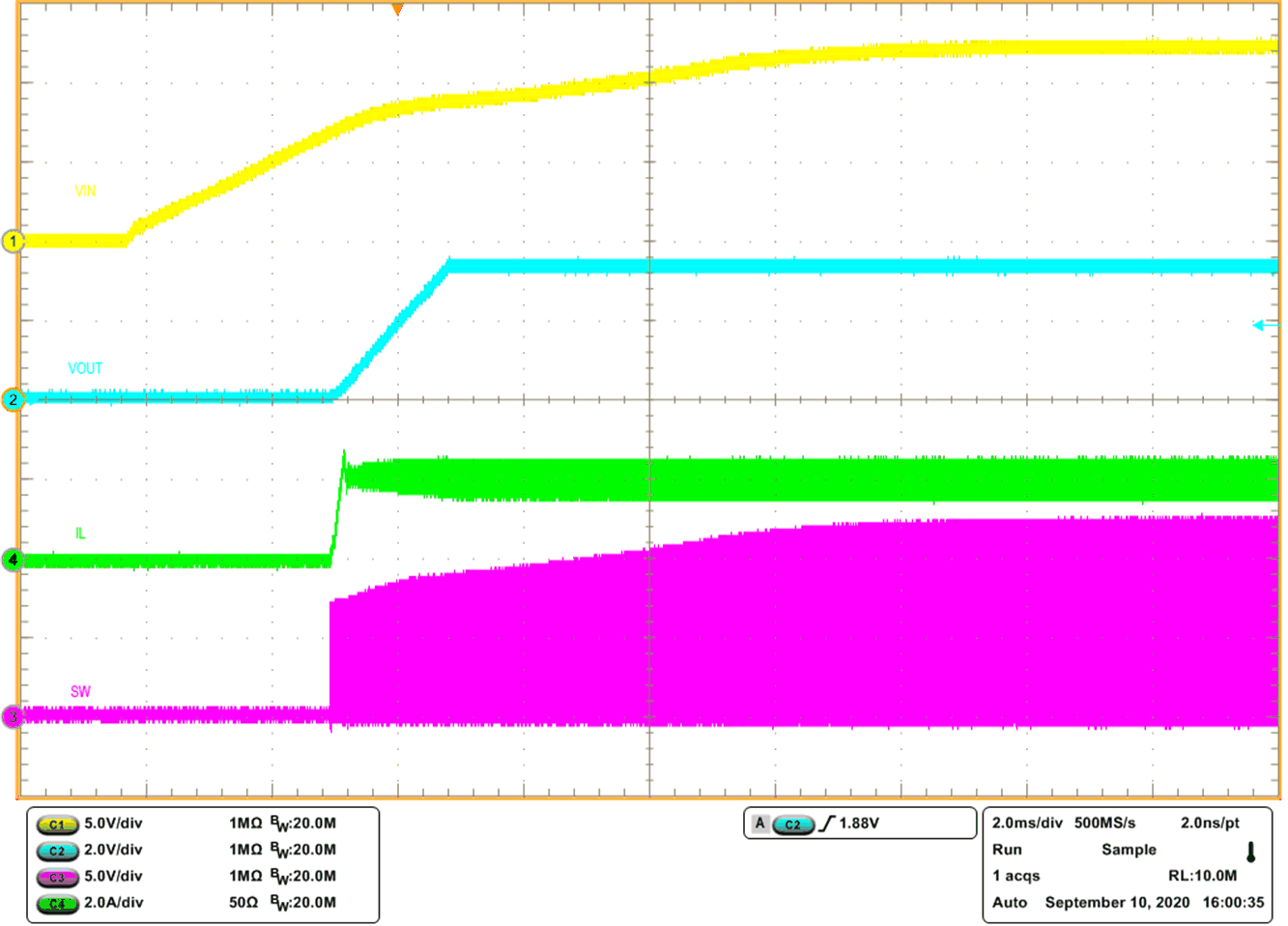 Figure 8-16 Start-Up Relative to VIN
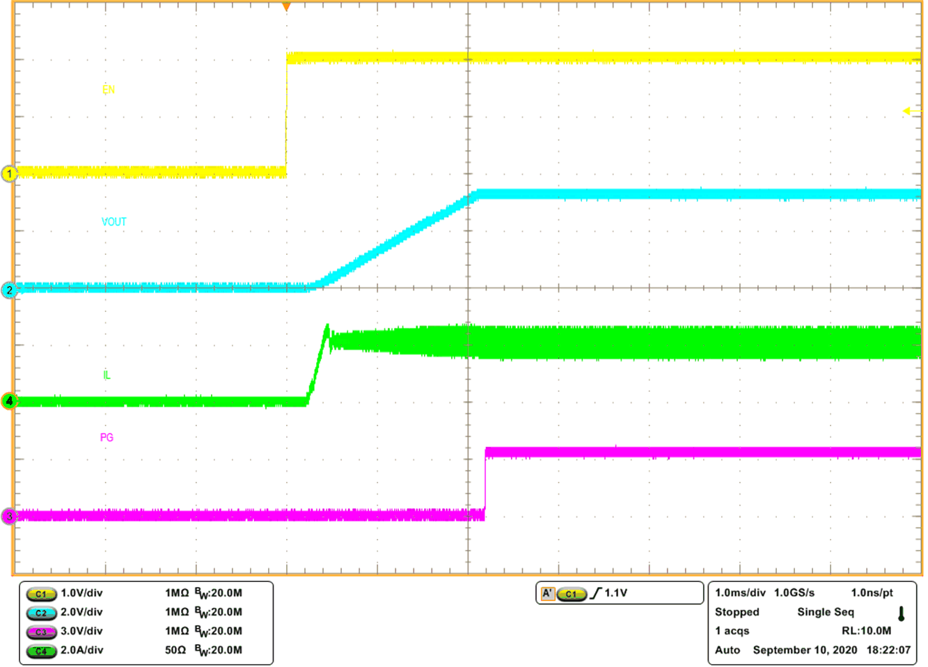 Figure 8-18 Enable Relative to EN
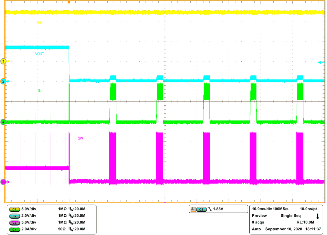 Figure 8-20 Output Short Protection
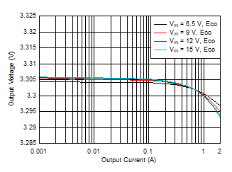 Figure 8-3 Load
Regulation
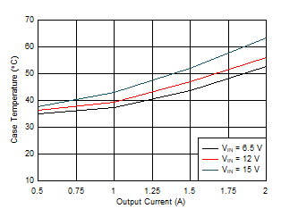 Figure 8-5 Case
Temperature Rise vs Load Current
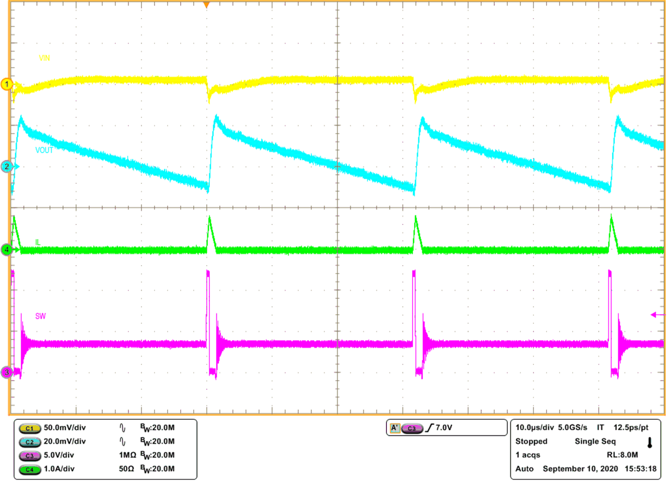 Figure 8-7 Steady State Waveforms, IOUT = 0.02
A
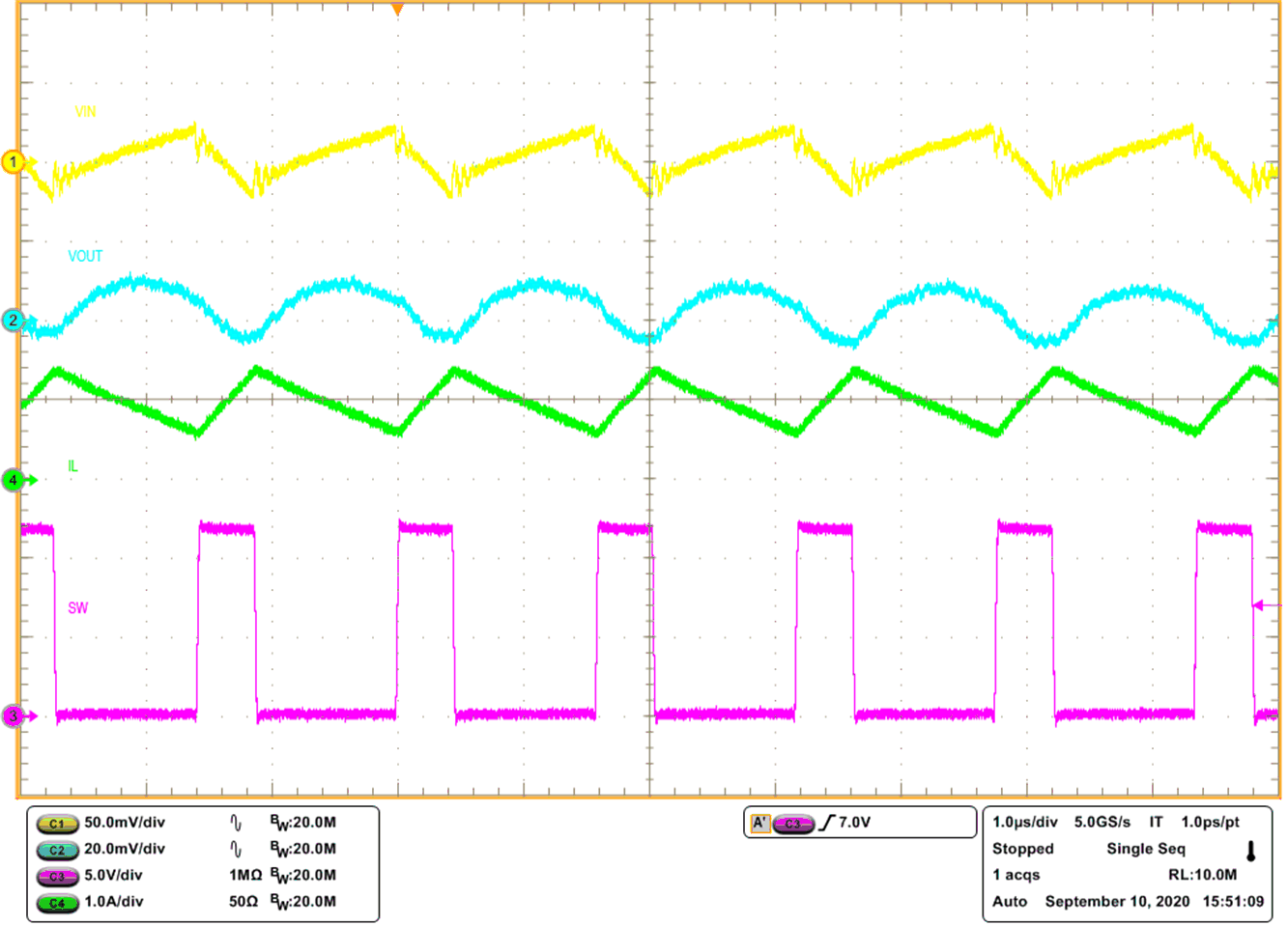 Figure 8-9 Steady State Waveforms, IOUT = 1 A
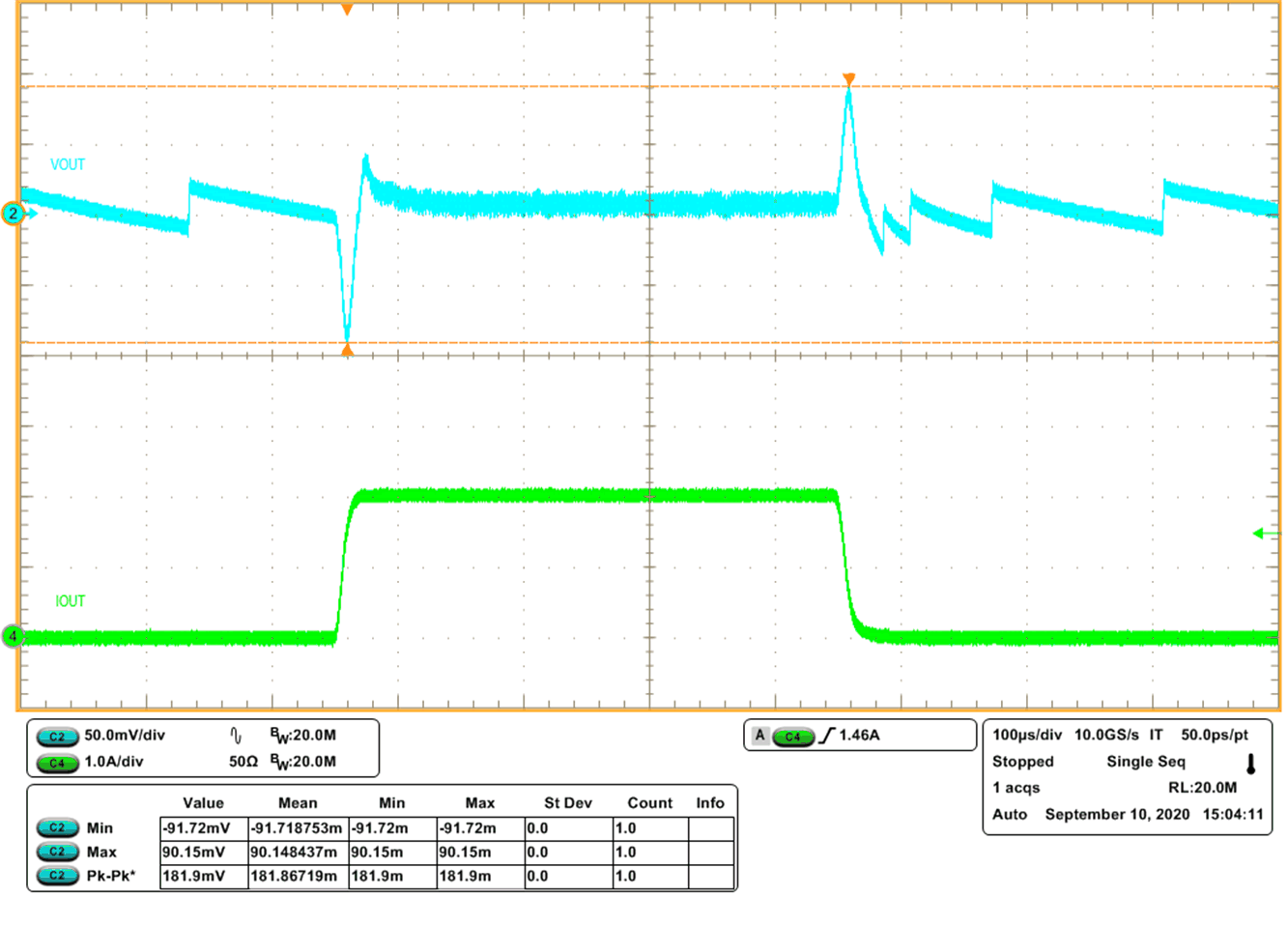 Figure 8-11 Transient Response 0 to 2 A with Slew Rate of 0.25 A/μs (Eco-mode)
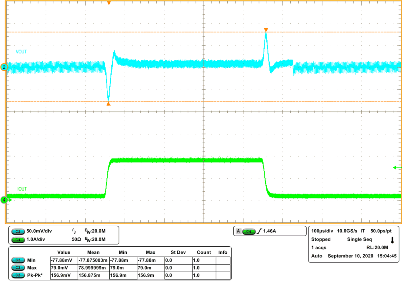 Figure 8-13 Transient Response 0.2 to 1.8 A with Slew Rate of 0.25 A/μs
(Eco-Mode)
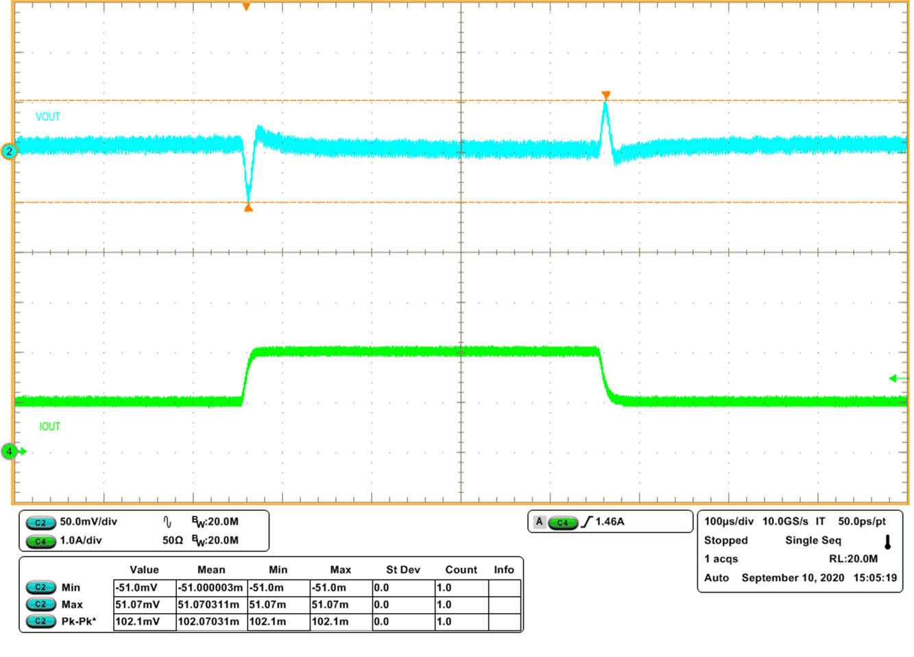 Figure 8-15 Transient Response 1 to 2 A with Slew Rate of 0.25 A/μs
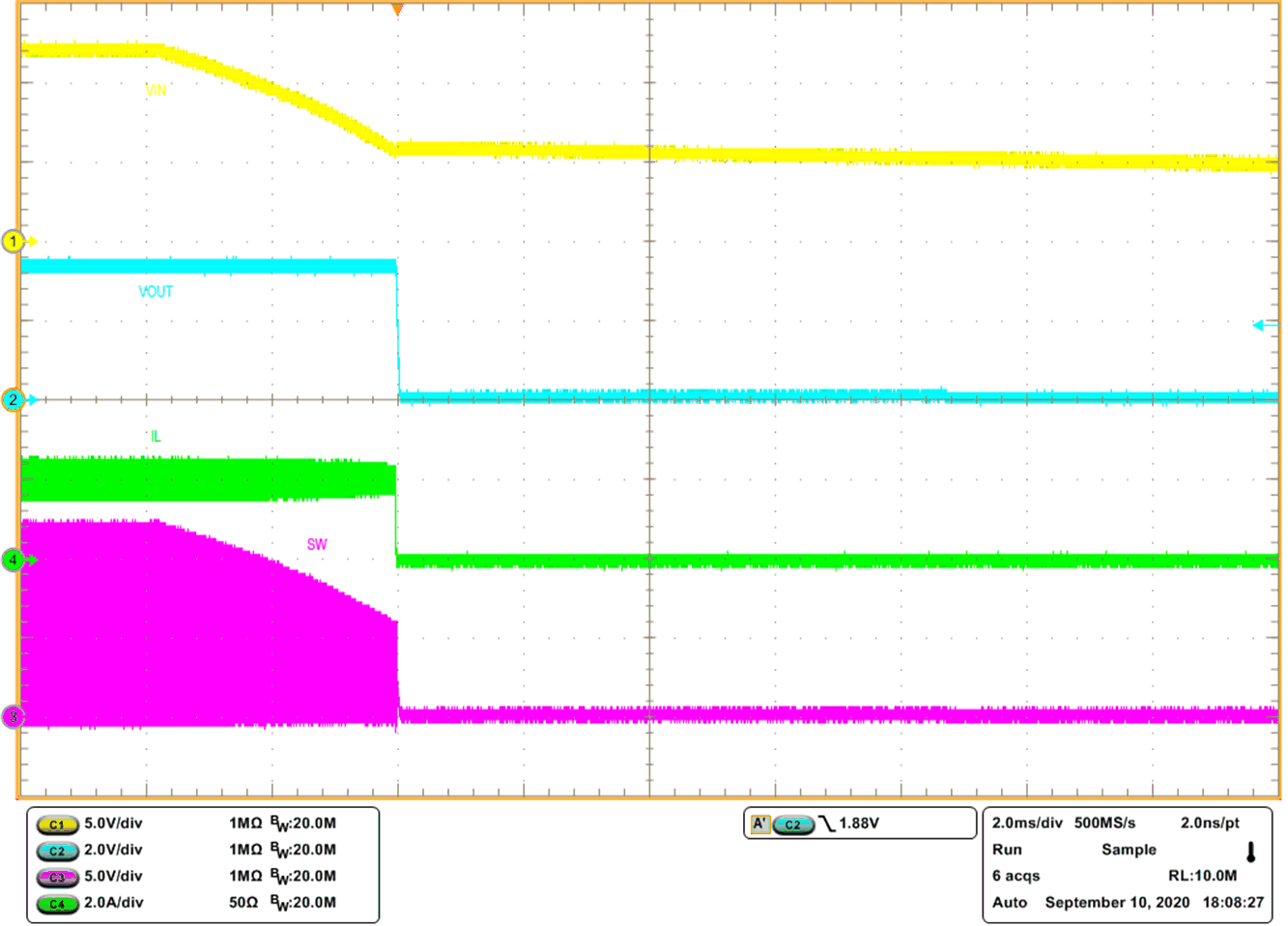 Figure 8-17 Shutdown Relative to VIN
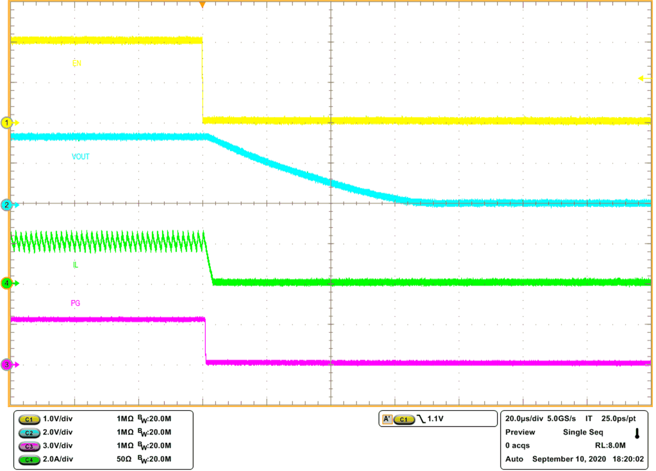 Figure 8-19 Disable Relative to EN
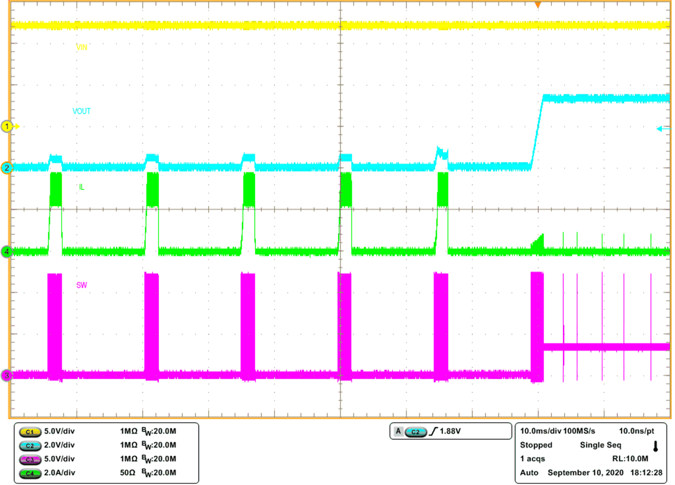 Figure 8-21 Output Short Recovery