SLUSDX0A September 2020 – August 2021 TPS562211
PRODUCTION DATA
- 1 Features
- 2 Applications
- 3 Description
- 4 Revision History
- 5 Pin Configuration and Functions
- 6 Specifications
-
7 Detailed Description
- 7.1 Overview
- 7.2 Functional Block Diagram
- 7.3
Feature Description
- 7.3.1 Advanced Emulated Current Mode Control
- 7.3.2 Mode Selection and PG/SS Pin Function Configuration
- 7.3.3 Power Good (PG)
- 7.3.4 Soft Start and Pre-Biased Soft Start
- 7.3.5 Output Discharge through PG/SS Pin
- 7.3.6 Precise Enable and Adjusting Undervoltage Lockout
- 7.3.7 Overcurrent Limit and Undervoltage Protection
- 7.3.8 Overvoltage Protection
- 7.3.9 Thermal Shutdown
- 7.4 Device Functional Modes
- 8 Application and Implementation
- 9 Power Supply Recommendations
- 10Layout
- 11Device and Documentation Support
- 12Mechanical, Packaging, and Orderable Information
Package Options
Mechanical Data (Package|Pins)
- DRL|8
Thermal pad, mechanical data (Package|Pins)
Orderable Information
7.4.6 On-Time Extension for Large Duty Cycle Operation
Minimum on time, TON_MIN, is the smallest duration of time that the high-side MOSFET can be on. TON_MIN is typically 45 ns in the device. Minimum off time, TOFF_MIN, is the smallest duration that the high-side MOSFET can be off. TOFF_MIN is typically 105 ns in the device. In CCM operation, TON_MIN and TOFF_MIN limit the voltage conversion range given a fixed switching frequency.
The minimum duty cycle allowed is:

The maximum duty cycle allowed is:

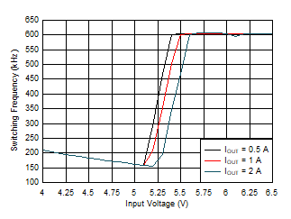
In the device, a frequency foldback scheme is employed to extend the maximum duty cycle when TOFF_MIN is reached. The switching frequency decreases once longer duty cycle is needed under low VIN conditions. With the duty increased, the on-time is extended until up to the maximum on-time, 6 μs. Wide range of frequency foldback allows the device output voltage stay in regulation with a much lower supply voltage VIN. This leads to a lower effective dropout voltage.
Given an output voltage, the maximum operation supply voltage can be found by:

At lower supply voltage, the switching frequency decreases once TOFF_MIN is triggered. The minimum VIN without frequency foldback can be approximated by:

Taking considerations of power losses in the system with heavy load operation, VIN_MAX is higher than the result calculated in Equation 9. With frequency foldback, VIN_VIN is lowered by decreased fSW, as shown in Figure 7-4.
 Figure 7-4 Frequency Foldback at Dropout
(VOUT = 5 V)