-
TPS562212 4.2-V to 18-V Input, 2-A Synchronous Buck Converter in a SOT-5X3 Package
- 1 Features
- 2 Applications
- 3 Description
- 4 Revision History
- 5 Pin Configuration and Functions
- 6 Specifications
-
7 Detailed Description
- 7.1 Overview
- 7.2 Functional Block Diagram
- 7.3
Feature Description
- 7.3.1 Advanced Emulated Current Mode Control
- 7.3.2 Mode Selection and PG/SS Pin Function Configuration
- 7.3.3 Power Good (PG)
- 7.3.4 Soft Start and Pre-Biased Soft Start
- 7.3.5 Output Discharge Through PG/SS Pin
- 7.3.6 Precise Enable and Adjusting Undervoltage Lockout
- 7.3.7 Overcurrent Limit and Undervoltage Protection
- 7.3.8 Overvoltage Protection
- 7.3.9 Thermal Shutdown
- 7.4 Device Functional Modes
- 8 Application and Implementation
- 9 Power Supply Recommendations
- 10Layout
- 11Device and Documentation Support
- 12Mechanical, Packaging, and Orderable Information
- IMPORTANT NOTICE
Package Options
Mechanical Data (Package|Pins)
- DRL|8
Thermal pad, mechanical data (Package|Pins)
Orderable Information
TPS562212 4.2-V to 18-V Input, 2-A Synchronous Buck Converter in a SOT-5X3 Package
1 Features
- 4.2-V to 18-V input voltage
- 0.6-V to 7-V output voltage
- Up to 2-A continuous output current
- 45-ns minimum switching on time
- 98% maximum duty cycle
- High efficiency
- Integrated 66-mΩ and 33-mΩ MOSFETs
- 120-μA typical quiescent current
- Highly flexible and easy to use
- Selectable Eco-mode or FCCM operation
- Selectable power-good indicator or external soft start
- Precise enable input
- High accuracy
- ±1% (25°C) reference voltage accuracy
- ±8.5% switching frequency tolerance
- Small solution size
- Internal compensation for ease of use
- SOT-5X3 package
- Minimum external components
- Cycle-by-cycle current limit for both high-side and low-side MOSFETs
- Non-latched OVP, UVP, UVLO, and TSD protections
- Create a custom design using TPS562212 with the WEBENCH® Power Designer
2 Applications
3 Description
The TPS562212 is a cost-effective and highly flexible synchronous buck converter that provides selectable Eco-mode operation or FCCM (force continuous conduction mode) operation. A selectable power-good indicator or external soft start is also configurable through the MODE pin. Power sequencing is possible by correctly configuring the Enable pin, power-good indicator, or external soft start. A wide input voltage range of 4.2 V to 18 V supports a wide variety of common input rails like 12 V and 15 V. It supports up to 2-A continuous output current at output voltages between 0.6 V and 7 V.
The device provides fast transient response with true fixed switching frequency through the use of the Advanced Emulated Current Mode (AECM) control topology. With internal smart loop bandwidth control, the device provides fast transient response over a wide output voltage range without the need for external compensation.
Cycle-by-cycle current limit on the high-side peak current protects the device in overload situations and is enhanced by a low-side valley current limit, which prevents current runaway. Hiccup mode would be triggered under overvoltage protection (OVP), undervoltage protection (UVP), UVLO protection, and thermal shutdown.
The device is available in a 1.6-mm × 2.1-mm SOT583 package.
| PART NUMBER | PACKAGE(1) | BODY SIZE (NOM) |
|---|---|---|
| TPS562212 | SOT-5X3 (8) | 1.6 mm × 2.1 mm |
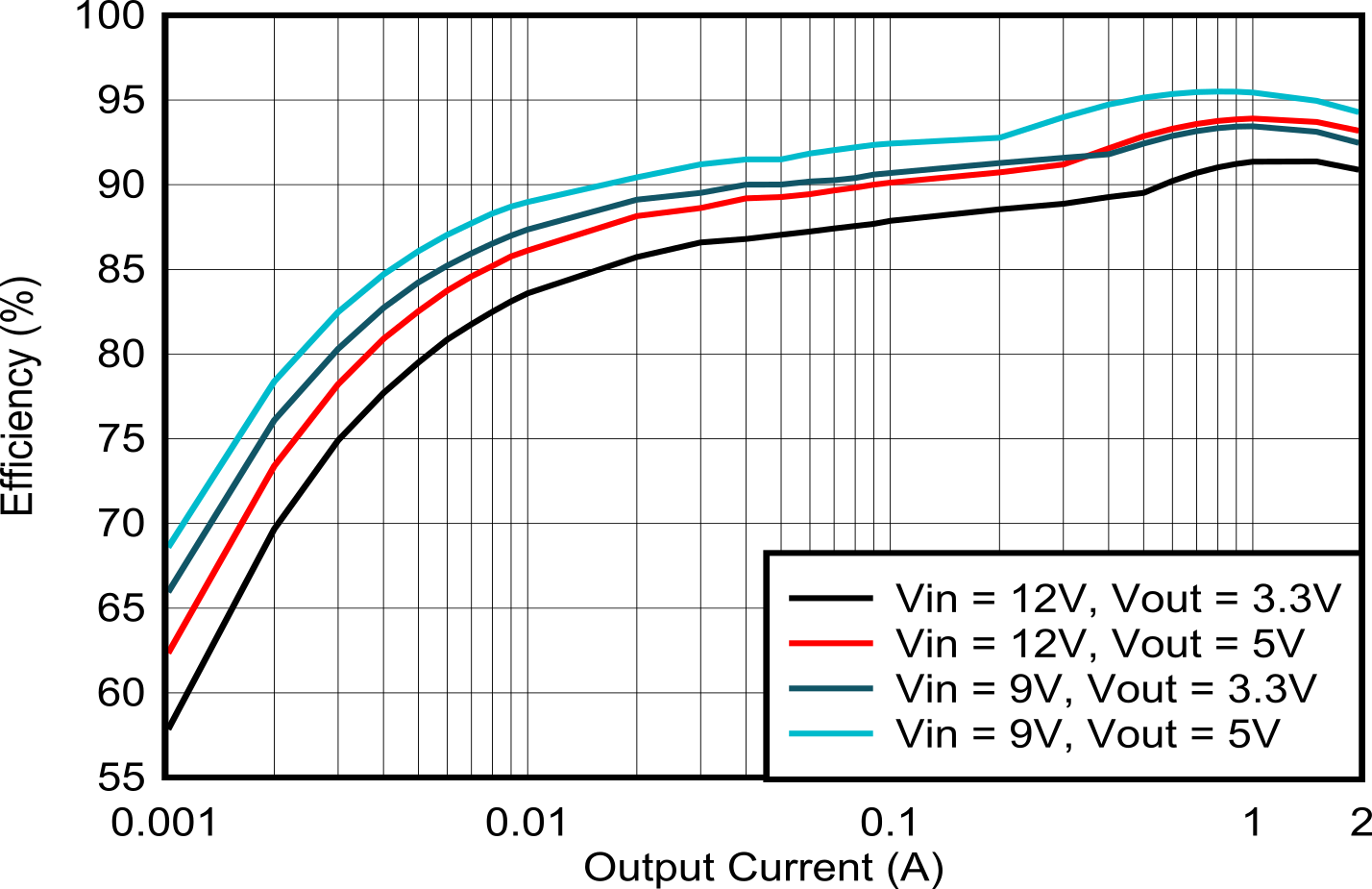
 Efficiency vs Output
Current
Efficiency vs Output
Current4 Revision History
| DATE | REVISION | NOTES |
|---|---|---|
| October 2021 | * | Initial Release |
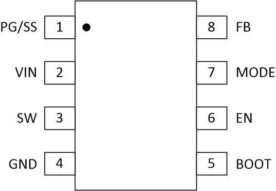
5 Pin Configuration and Functions
 8-Pin SOT-5X3
DRL Package (Top View)
8-Pin SOT-5X3
DRL Package (Top View)| PIN | I/O(1) | DESCRIPTION | |
|---|---|---|---|
| NAME | NO. | ||
| PG/SS | 1 | I/O | This pin can be selected as a
power-good function or soft-start function, depending on the device
MODE pin configuration.
|
| VIN | 2 | P | Input voltage supply pin for the control circuitry. Connect the input decoupling capacitors between VIN and GND. |
| SW | 3 | P | Switch node terminal. Connect the output inductor to this pin. |
| GND | 4 | G | GND terminal for the controller circuit and the internal circuitry |
| BOOT | 5 | P | Supply input for the high-side MOSFET gate drive circuit. Connect a 0.1-µF capacitor between the BOOT and SW pins. |
| EN | 6 | I/O | Enable input control. Driving EN high or leaving this pin floating enables the converter. An external resistor divider can be used to imply an adjustable VIN UVLO function. |
| MODE | 7 | I/O | Device operation mode in light load (Eco-mode operation or FCCM operation) and pin 1 function (PG/SS) selection pin. Connect a resistor from MODE to GND to configure the device according to Table 7-1. |
| FB | 8 | I | Converter feedback input. Connect to the output voltage with a feedback resistor divider. |