SLVSD90B December   2015  – September 2024 TPS563201 , TPS563208

PRODUCTION DATA  

  1.   1
  2. Features
  3. Applications
  4. Description
  5. Pin Configuration and Functions
  6. Specifications
    1. 5.1 Absolute Maximum Ratings
    2. 5.2 ESD Ratings
    3. 5.3 Recommended Operating Conditions
    4. 5.4 Thermal Information
    5. 5.5 Electrical Characteristics
    6. 5.6 Typical Characteristics
  7. Detailed Description
    1. 6.1 Overview
    2. 6.2 Functional Block Diagram
    3. 6.3 Feature Description
      1. 6.3.1 Adaptive On-Time Control and PWM Operation
      2. 6.3.2 Pulse Skip Control (TPS563201)
      3. 6.3.3 Soft Start and Pre-Biased Soft Start
      4. 6.3.4 Current Protection
      5. 6.3.5 Undervoltage Lockout (UVLO) Protection
      6. 6.3.6 Thermal Shutdown
    4. 6.4 Device Functional Modes
      1. 6.4.1 Normal Operation
      2. 6.4.2 Eco-mode Operation
      3. 6.4.3 Standby Operation
  8. Application and Implementation
    1. 7.1 Application Information
    2. 7.2 Typical Application
      1. 7.2.1 Design Requirements
      2. 7.2.2 Detailed Design Procedure
        1. 7.2.2.1 Custom Design with WEBENCH® Tools
        2. 7.2.2.2 Output Voltage Resistors Selection
        3. 7.2.2.3 Output Filter Selection
        4. 7.2.2.4 Input Capacitor Selection
        5. 7.2.2.5 Bootstrap Capacitor Selection
      3. 7.2.3 Application Curves
    3. 7.3 Power Supply Recommendations
    4. 7.4 Layout
      1. 7.4.1 Layout Guidelines
      2. 7.4.2 Layout Example
  9. Device and Documentation Support
    1. 8.1 Device Support
      1. 8.1.1 Development Support
        1. 8.1.1.1 Custom Design with WEBENCH® Tools
    2. 8.2 Receiving Notification of Documentation Updates
    3. 8.3 Support Resources
    4. 8.4 Trademarks
    5. 8.5 Electrostatic Discharge Caution
    6. 8.6 Glossary
  10. Revision History
  11. 10Mechanical, Packaging, and Orderable Information
    1. 10.1 Tape and Reel Information

Package Options

Refer to the PDF data sheet for device specific package drawings

Mechanical Data (Package|Pins)
  • DDC|6
Thermal pad, mechanical data (Package|Pins)
Orderable Information

Application Curves

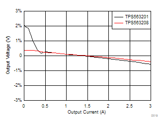
TPS563201 TPS563208 TPS563201 and TPS563208 Load Regulation, VIN = 5 V
Figure 7-2 TPS563201 and TPS563208 Load Regulation, VIN = 5 V
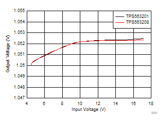
TPS563201 TPS563208 TPS563201 and TPS563208 Line Regulation
IOUT of TPS563201: 1 A
IOUT of TPS563208: 10 mA
Figure 7-4 TPS563201 and TPS563208 Line Regulation
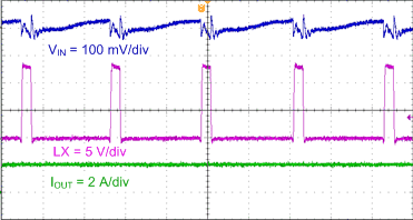
TPS563201 TPS563208 TPS563201 Input Voltage Ripple
800 ns/div
Figure 7-6 TPS563201 Input Voltage Ripple
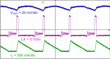
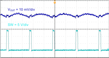
TPS563201 TPS563208 TPS563201 Output Voltage Ripple, Iout = 0.25 A
1 µs/div
Figure 7-8 TPS563201 Output Voltage Ripple, Iout = 0.25 A
TPS563201 TPS563208 TPS563208 Output Voltage Ripple, IOUT = 0 A
800 ns/div
Figure 7-10 TPS563208 Output Voltage Ripple, IOUT = 0 A
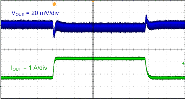
TPS563201 TPS563208 TPS563201 Transient Response, 0.75 to 2.25 A
100 µs/div
Figure 7-12 TPS563201 Transient Response, 0.75 to 2.25 A
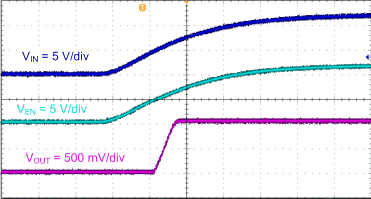
TPS563201 TPS563208 TPS563201 Start Up Relative to VI
2 ms/div
Figure 7-14 TPS563201 Start Up Relative to VI
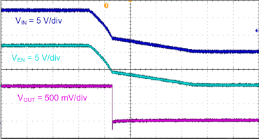
TPS563201 TPS563208 TPS563201 Shutdown Relative to VI
10 ms/div
Figure 7-16 TPS563201 Shutdown Relative to VI
TPS563201 TPS563208 TPS563201 and TPS563208 Load Regulation, VIN = 12 V
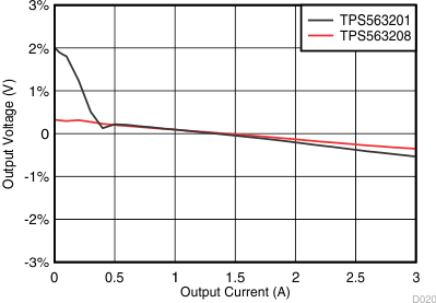
Figure 7-3 TPS563201 and TPS563208 Load Regulation, VIN = 12 V
TPS563201 TPS563208 TPS563201 Efficiency
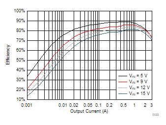
Figure 7-5 TPS563201 Efficiency
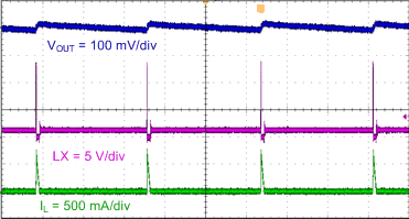
TPS563201 TPS563208 TPS563201 Output Voltage Ripple, 10 mA
20 µs/div
Figure 7-7 TPS563201 Output Voltage Ripple, 10 mA
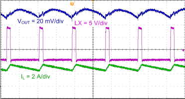
TPS563201 TPS563208 TPS563201 Output Voltage Ripple, Iout = 2 A
1 µs/div
Figure 7-9 TPS563201 Output Voltage Ripple, Iout = 2 A
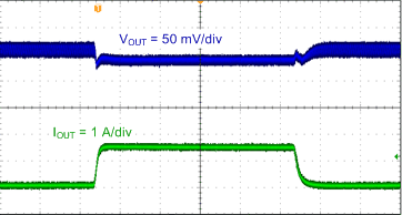
TPS563201 TPS563208 TPS563201 Transient Response, 0.1 to 1.5 A
100 µs/div
Figure 7-11 TPS563201 Transient Response, 0.1 to 1.5 A
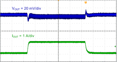
TPS563201 TPS563208 TPS563208 Transient Response 0.1 to 2 A
100 µs/div
Figure 7-13 TPS563208 Transient Response 0.1 to 2 A
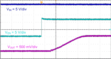
TPS563201 TPS563208 TPS563201 Start-Up Relative to EN
400 µs/div
Figure 7-15 TPS563201 Start-Up Relative to EN
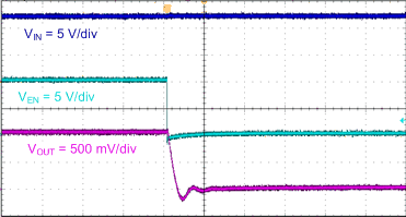
TPS563201 TPS563208 TPS563201 Shutdown Relative to EN
100 µs/div
Figure 7-17 TPS563201 Shutdown Relative to EN