SLVSD90B December 2015 – September 2024 TPS563201 , TPS563208
PRODUCTION DATA
- 1
- 1 Features
- 2 Applications
- 3 Description
- 4 Pin Configuration and Functions
- 5 Specifications
- 6 Detailed Description
- 7 Application and Implementation
- 8 Device and Documentation Support
- 9 Revision History
- 10Mechanical, Packaging, and Orderable Information
Package Options
Refer to the PDF data sheet for device specific package drawings
Mechanical Data (Package|Pins)
- DDC|6
Thermal pad, mechanical data (Package|Pins)
Orderable Information
7.2 Typical Application
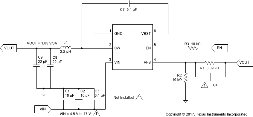
The application schematic in Figure 7-1 was developed to meet the previous requirements. This circuit is available as the evaluation module (EVM). The sections provide the design procedure.
Figure 7-1 shows the TPS563201 and TPS563208 4.5-V to 17-V input, 1.05-V output converter schematics.
 Figure 7-1 TPS563201 and TPS563208 1.05-V/3-A Reference Design