SLVSCV3B March 2015 – June 2015 TPS566250
PRODUCTION DATA.
- 1 Features
- 2 Applications
- 3 Description
- 4 Simplified Schematic
- 5 Revision History
- 6 Pin Configuration and Functions
- 7 Specifications
- 8 Detailed Description
- 9 Applications and Implementation
- 10Power Supply Recommendations
- 11Layout
- 12Device and Documentation Support
- 13Mechanical, Packaging, and Orderable Information
Package Options
Mechanical Data (Package|Pins)
- DDA|8
Thermal pad, mechanical data (Package|Pins)
- DDA|8
Orderable Information
9 Applications and Implementation
NOTE
Information in the following applications sections is not part of the TI component specification, and TI does not warrant its accuracy or completeness. TI’s customers are responsible for determining suitability of components for their purposes. Customers should validate and test their design implementation to confirm system functionality.
9.1 Application Information
The devices are synchronous step down DC-DC converters rated at different output currents whose output voltage can be dynamically scaled by sending commands over an I2C interface. This section discusses the design of the external components to complete the power supply design by using a typical application as a reference.
9.2 Typical Application
 Figure 17. Typical Application Schematic
Table 4. Components
| REFERENCE DESIGNATOR | PART NUMBER | MANUFACTURER |
|---|---|---|
| L1 | 744 314 150 | Wurth Electronics |
| C6 , C7 | C1210C226K9RACTU | Kemet |
9.2.1 Design Requirements
For this design example, use the parameters shown in Table 5.
Table 5. Design Example
| DESIGN PARAMETER | EXAMPLE VALUE |
|---|---|
| Input voltage | 12 V |
| Output voltage | 1.1 V |
| Transient response, 0 A – 6 A load step | ΔVOUT = ±5% |
| Output voltage ripple | 25 mV |
| Input ripple voltage | 400 mV |
| Output current rating | 6 A |
| Operating Frequency | 650 kHz |
9.2.2 Detailed Design Procedure
9.2.2.1 Output Voltage Resistors Selection
The output voltage is set with a resistor divider from the output node to the FB pin. It is recommended to use 1% tolerance or better divider resistors. Use 1.37 kΩ for R1 and 1.65 kΩ for R2.

9.2.2.2 Output Filter Selection
The output filter used with the TPS566250 is an LC circuit. This LC filter has double pole at:

At low frequencies, the overall loop gain is set by the output set-point resistor divider network and the internal gain of the device. The low frequency phase is 180 degrees. At the output filter pole frequency, the gain rolls off at a –40 dB per decade rate and the phase drops rapidly. D-CAP2™ introduces a high frequency zero that reduces the gain roll off to –20 dB per decade and increases the phase to 90 degrees one decade above the zero frequency. The inductor and capacitor selected for the output filter must be selected so that the double pole of Equation 4 is located below the high frequency zero but close enough that the phase boost provided be the high frequency zero provides adequate phase margin for a stable circuit. To meet this requirement use the values recommended in Table 6.
Table 6. Recommended Component Values
| Output Voltage (V) | R1 (kΩ) | R2 (kΩ) | C4 (pF)(1) | L1 (µH) | C67 (µF) | ||||
|---|---|---|---|---|---|---|---|---|---|
| MIN | TYP | MAX | MIN | TYP | MAX | ||||
| 1 | 1.37 | 1.65 | 1.5 | 22 - 68 | |||||
| 1.1 (Default) | 1.37 | 1.65 | 1.5 | 22 - 68 | |||||
| 1.2 | 1.37 | 1.65 | 1.5 | 22 - 68 | |||||
| 1.5 | 1.37 | 1.65 | 1.5 | 22 - 68 | |||||
| 1.8 | 1.37 | 1.65 | 1.5 | 22 - 68 | |||||
The inductor peak-to-peak ripple current, peak current and RMS current are calculated using Equation 5, Equation 6 and Equation 7. The inductor saturation current rating must be greater than the calculated peak current and the RMS or heating current rating must be greater than the calculated RMS current. For the calculations, use 500 kHz as the switching frequency, fSW. Make sure the chosen inductor is rated for the peak current of Equation 6 and the RMS current of Equation 7.


The capacitor value and ESR determines the amount of output voltage ripple. The TPS566250 is intended for use with ceramic or other low ESR capacitors. Recommended values range from 22 µF to 68 µF.
9.2.2.3 Input Capacitor Selection
The TPS566250 requires an input decoupling capacitor and a bulk capacitor depending on the application. A ceramic capacitor of 10 µF or above is recommended for the decoupling capacitor. Additionally, a 0.1-µF ceramic capacitor from VIN to GND is also recommended to improve the stability and reduce the SW node overshoots. The capacitors voltage rating needs to be greater than the maximum input voltage.
9.2.2.4 Bootstrap Capacitor Selection
The 0.1-µF ceramic capacitors must be connected between the BOOT to SW pins for proper operation. It is recommended to use ceramic capacitors with a dielectric of X5R or better.
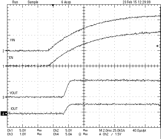
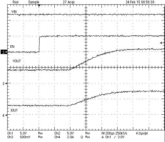
9.2.3 Application Performance Curves
VIN = 12 V, VOUT = 1.1 V, TA = 25°C, unless otherwise specified.

| VIN = 12 V |

| VOUT = 0.6 V |


(Inductor Current)


| VOUT = 1.87 V |

| VOUT = 1.1 V |


(Inductor Current)


