SLVSCV3B March 2015 – June 2015 TPS566250
PRODUCTION DATA.
- 1 Features
- 2 Applications
- 3 Description
- 4 Simplified Schematic
- 5 Revision History
- 6 Pin Configuration and Functions
- 7 Specifications
- 8 Detailed Description
- 9 Applications and Implementation
- 10Power Supply Recommendations
- 11Layout
- 12Device and Documentation Support
- 13Mechanical, Packaging, and Orderable Information
Package Options
Mechanical Data (Package|Pins)
- DDA|8
Thermal pad, mechanical data (Package|Pins)
- DDA|8
Orderable Information
7 Specifications
7.1 Absolute Maximum Ratings
over operating free-air temperature range (unless otherwise noted) (1)(2)| MIN | MAX | UNIT | |||
|---|---|---|---|---|---|
| Input voltage range | VIN, EN | –0.3 | 19 | V | |
| BOOT | –0.3 | 25 | |||
| BOOT (10ns transient) | –0.3 | 27 | |||
| BOOT (vs SW) | –0.3 | 6.5 | |||
| FB, SDA, SCL | –0.3 | 3.6 | |||
| SW | –2 | 19 | |||
| SW (10ns transient) | –3.5 | 21 | |||
| Operating Junction temperature, TJ | –40 | 150 | °C | ||
| Storage temperature, TSTG | –55 | 150 | °C | ||
(1) These are stress ratings only, which do not imply functional operation of the device at these or any other conditions beyond those indicated under Recommended Operating Conditions.
(2) All voltages are with respect to IC GND terminal.
7.2 ESD Ratings
| VALUE | UNIT | |||
|---|---|---|---|---|
| V(ESD) | Electrostatic discharge | Human-body model (HBM), per ANSI/ESDA/JEDEC JS-001(1) | ±2000 | V |
| Charged-device model (CDM), per JEDEC specification JESD22-C101(2) | ±500 | |||
(1) JEDEC document JEP155 states that 500-V HBM allows safe manufacturing with a standard ESD control process.
(2) JEDEC document JEP157 states that 250-V CDM allows safe manufacturing with a standard ESD control process.
7.3 Recommended Operating Conditions
over operating free-air temperature range (unless otherwise noted)| MIN | MAX | UNIT | |||
|---|---|---|---|---|---|
| VIN | Supply input voltage range | 4.5 | 17 | V | |
| Input voltage range | BOOT | –0.1 | 23 | ||
| BOOT (10 ns transient) | –0.1 | 26 | |||
| BOOT (vs SW) | –0.1 | 6 | |||
| EN | –0.1 | 17 | |||
| FB, SDA, SCL | –0.1 | 3.3 | |||
| SW | –1.8 | 17 | |||
| SW (10 ns transient) | –3.5 | 20 | |||
| TJ | Operating junction temperature range | –40 | 150 | °C | |
7.4 Thermal Information
| THERMAL METRIC(1) | TPS566250 | UNIT | |
|---|---|---|---|
| DDA (8) | |||
| RθJA | Junction-to-ambient thermal resistance | 42.1 | °C/W |
| RθJCtop | Junction-to-case (top) thermal resistance | 55.7 | |
| RθJB | Junction-to-board thermal resistance | 24.9 | |
| ψJT | Junction-to-top characterization parameter | 9.5 | |
| ψJB | Junction-to-board characterization parameter | 24.9 | |
| RθJCbot | Junction-to-case (bottom) thermal resistance | 3.5 | |
(1) For more information about traditional and new thermal metrics, see the IC Package Thermal Metrics application report, SPRA953.
7.5 Electrical Characteristics
Over operating junction temperature range, VIN = 12 V (Unless otherwise noted)| PARAMETER | CONDITIONS | MIN | TYP | MAX | UNIT | |
|---|---|---|---|---|---|---|
| SUPPLY VOLTAGE | ||||||
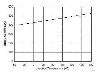
| IIN | VIN supply current | TA = 25°C, EN = 5 V, FB = 0.7 V (non switching) | 450 | 525 | µA | |
| I(VINSDN) | VIN shutdown current | TA = 25°C, EN = 0 V | 6.5 | 10 | µA | |
| LOGIC THRESHOLD | ||||||
| V(ENH) | EN H-level threshold voltage | 1.1 | 1.6 | V | ||
| V(ENL) | EN L-level threshold voltage | 0.6 | 0.94 | V | ||
| Hystersis | 160 | mV | ||||
| R(EN) | EN pin resistance to GND | V(EN) = 12 V | 225 | 350 | 800 | kΩ |
| FEEDBACK VOLTAGE | ||||||
| V(FB) | FB voltage | TA = 0°C to 85°C VOUT = 1.1 V, Upper/lower feedback resistors: 1.37 kΩ / 1.65 kΩ |
–1.6% | 0 | 1.6% | |
| TA = 25°C, VOUT = 1.1 V, IOUT = 10 mA, pulse skipping | 0.606 | V | ||||
| TA = 25°C, VOUT = 1.1 V, continuous current mode | 0.594 | 0.6 | 0.606 | V | ||
| MOSFET | ||||||
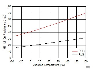
| rDS(on)H | High side switch resistance | BOOT - SW = 5.5 V | 44 | 74 | mΩ | |
| rDS(on)L | Low side switch resistance | VIN = 12 V | 23 | 35 | mΩ | |
| Discharge FET | 200 | Ω | ||||
| ON-TIME TIMER CONTROL | ||||||
| fsw | Switching frequency | LOUT = 1.5 µH, COUT = 22 µF x 2, VOUT = 1.1 V | 650 | kHz | ||
| CURRENT LIMIT | ||||||
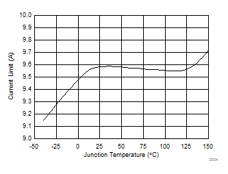
| IOCL | Valley current limit | LOUT = 1.5 µH, VOUT = 1.1 V, VIN = 12 V | 7.6 | 9.5 | 11.4 | A |
| Reverse valley current limit | LOUT = 1.5 µH, VOUT = 1.1 V | 1.5 | 4.5 | 7 | A | |
| OUTPUT UNDERVOLTAGE PROTECTION | ||||||
| V(UVP) | Output UVP trip threshold | UVP detect (H > L) | 65% | |||
| THERMAL SHUTDOWN | ||||||
| TSDN | Thermal shutdown Threshold | Shutdown temperature(1) | 165 | °C | ||
| Hysteresis(1) | 15 | °C | ||||
| UVLO | ||||||
| UVLO | UVLO Threshold | VIN rising voltage | 3.26 | 3.75 | 4.05 | V |
| Hysteresis VIN voltage | 0.13 | 0.33 | 0.48 | V | ||
| PGOOD VIA I2C | ||||||
| V(PGOODTH) | PGOOD threshold | FB falling (fault) VO = 1.1 V | 80% | |||
| FB rising (good) VO = 1.1 V | 85% | |||||
| FB rising (fault) VO = 1.1 V | 125% | |||||
| FB falling (good) VO = 1.1 V | 120% | |||||
| SERIAL INTERFACE(1)(2)(3) | ||||||
| VIL | LOW level input voltage | 0.6 | V | |||
| VIH | HIGH level input voltage | 1.85 | V | |||
| Vhys | Hysteresis of schmitt trigger inputs | 0.11 | V | |||
| VOL | LOW level output voltage (Open drain, 3 mA sink current) |
0.4 | V | |||
| fSCL | SCL clock frequency | 400 | kHz | |||
| Cb | Capacitive load for each bus line | 400 | pF | |||
(1) Specified by design. Not production tested.
(2) Refer to Figure 1 for I2C Timing Definitions
(3) Cb = capacitance of bus line in pF
7.6 Timing Requirements
| MIN | TYP | MAX | UNIT | |||
|---|---|---|---|---|---|---|
| ON-TIME TIMER CONTROL | ||||||
| ton | SW On time | VIN = 12 V, VOUT = 1.1 V | 165 | ns | ||
| toff | SW Minimum off time | TA = 25 °C, FB = 0.5 V | 275 | 325 | ns | |
| SOFT START | ||||||
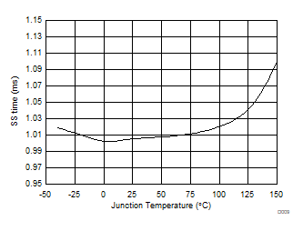
| tSS | Soft start time | Internal soft start time | 0.7 | 1 | 1.3 | ms |
| OUTPUT UNDERVOLTAGE PROTECTION | ||||||
| t(UVPDEL) | Hiccup delay time (power into short) | 1.3 | ms | |||
| t(UVPEN) | Hiccup off time before restart | 10 | ms | |||
| SERIAL INTERFACE(1)(2)(3) | ||||||
| t(SP) | Pulse width of spikes suppressed by input filter | 32 | ns | |||
| t(HD;STA) | Hold time (repeated) START condition. | 0.6 | µs | |||
| tLOW | LOW period of SCL clock | 1.3 | µs | |||
| tHIGH | HIGH period of SCL clock | 0.6 | µs | |||
| t(SU;STA) | Set-up time for a repeated START condition | 0.6 | µs | |||
| t(HD;DAT) | Data Hold time | 50 | 900 | ns | ||
| t(SU;DAT) | Data set-up time | 100 | ns | |||
| tr | Rise time (SDA or SCL) | 20+0.1Cb(3) | 300 | ns | ||
| tf | Fall time (SDA or SCL) | 20+0.1Cb(3) | 300 | ns | ||
| t(SU;STO) | Set-up time for STOP condition | 0.6 | µs | |||
| t(BUF) | Bus free time between STOP and START condition | 1.3 | µs | |||
(1) Specified by design. Not production tested.
(2) Refer to Figure 1 below for I2C Timing Definitions
(3) Cb = capacitance of bus line in pF
 Figure 1. I2C Timing Definitions (reproduced from Phillips I2C spec Version 1.1)
7.7 Typical Characteristics
VIN = 12 V, TA = 25 °C, unless otherwise specified.


