SLVSCB6E November   2013  – December 2017 TPS56520 , TPS56720 , TPS56920 , TPS56C20

PRODUCTION DATA.  

  1. Features
  2. Applications
  3. Description
  4. Revision History
  5. Description (Continued)
  6. Pin Configuration and Functions
  7. Specifications
    1. 7.1 Absolute Maximum Ratings
    2. 7.2 ESD Ratings
    3. 7.3 Recommended Operating Conditions
    4. 7.4 Thermal Information
    5. 7.5 Electrical Characteristics
    6. 7.6 Timing Requirements
    7. 7.7 Switching Characteristics
    8. 7.8 Typical Characteristics
  8. Detailed Description
    1. 8.1 Overview
    2. 8.2 Functional Block Diagram
    3. 8.3 Feature Description
      1. 8.3.1 PWM Operation
      2. 8.3.2 PWM Frequency and Adaptive On-Time Control
      3. 8.3.3 VIN and Power VIN Terminals (VIN and PVIN)
      4. 8.3.4 Auto-Skip Eco-mode™ Control
      5. 8.3.5 Soft Start and Pre-Biased Soft Start
      6. 8.3.6 Power Good
      7. 8.3.7 Overcurrent Protection
      8. 8.3.8 UVLO Protection
    4. 8.4 Device Functional Modes
      1. 8.4.1 Operation at Light Loads
    5. 8.5 Programming
      1. 8.5.1 I2C Interface
      2. 8.5.2 I2C Protocol
      3. 8.5.3 I2C Chip Address Byte
    6. 8.6 Register Maps
      1. 8.6.1 I2C Register Address Byte
      2. 8.6.2 Output Voltage Registers
      3. 8.6.3 CheckSum Bit (VOUT Register Only)
      4. 8.6.4 Control Registers
      5. 8.6.5 Latchoff
  9. Applications and Implementation
    1. 9.1 Application Information
    2. 9.2 Typical Application
      1. 9.2.1 TPS56520, TPS56720 and TPS56920, 5-A, 7-A, and 9-A Converter
        1. 9.2.1.1 Design Requirements
        2. 9.2.1.2 Detailed Design Procedure
          1. 9.2.1.2.1 Output Voltage Resistors Selection
            1. 9.2.1.2.1.1 Output Filter Selection
          2. 9.2.1.2.2 Input Capacitor Selection
          3. 9.2.1.2.3 Bootstrap Capacitor Selection
          4. 9.2.1.2.4 VREG5 Capacitor Selection
      2. 9.2.2 TPS56520, TPS56720 and TPS56920 Application Performance Curves
      3. 9.2.3 TPS56C20 12-A Converter
        1. 9.2.3.1 Design Requirements
        2. 9.2.3.2 Design Procedure
        3. 9.2.3.3 TPS56C20 Application Performance Curves
  10. 10Power Supply Recommendations
  11. 11Layout
    1. 11.1 Layout Guidelines
    2. 11.2 Layout Example
  12. 12Device and Documentation Support
    1. 12.1 Device Support
      1. 12.1.1 Development Support
    2. 12.2 Documentation Support
      1. 12.2.1 Related Documentation
    3. 12.3 Related Links
    4. 12.4 Trademarks
    5. 12.5 Electrostatic Discharge Caution
    6. 12.6 Glossary
  13. 13Mechanical, Packaging, and Orderable Information

Package Options

Refer to the PDF data sheet for device specific package drawings

Mechanical Data (Package|Pins)
  • PWP|20
Thermal pad, mechanical data (Package|Pins)
Orderable Information

Layout

Layout Guidelines

  1. Keep the input switching current loop as small as possible. And avoid the input switching current through thermal Pad.
  2. Keep the SW node as physically small and short as possible to minimize parasitic capacitance and inductance and to minimize radiated emissions. Kelvin connections should be brought from the output to the feedback terminal of the device.
  3. Keep analog and non-switching components away from switching components.
  4. Make a single point connection from the signal ground to power ground.
  5. Do not allow switching current to flow under the device.
  6. Keep the pattern lines for VIN and PGND broad.
  7. Exposed pad of device must be connected to PGND with solder.
  8. VREG5 capacitor should be placed near the device, and connected to GND.
  9. Output capacitor should be connected to a broad pattern of the PGND.
  10. Voltage feedback loop should be as short as possible, and preferably with ground shield.
  11. Kelvin connections should be brought from the output to the feedback terminal of the device.
  12. Providing sufficient via is preferable for VIN, SW and PGND connection.
  13. PCB pattern for VIN, SW, and PGND should be as broad as possible.
  14. Input capacitors should be placed as near as possible to the device.
  15. The topside and the bottom side of the PCB should be filled with as much ground plane as possible that has an uninterrupted heat flow path. The ground plane should be made as large as possible. The PVIN cap should connect to PGND and the VIN cap should connect to GND.  
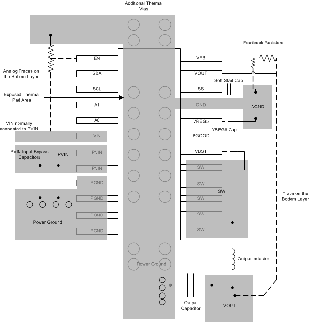
Layout Example

TPS56C20 TPS56920 TPS56720 TPS56520 layout2_slvscb6.gif Figure 57. TPS56X20 Board Layout