SLVSCB6E November 2013 – December 2017 TPS56520 , TPS56720 , TPS56920 , TPS56C20
PRODUCTION DATA.
- 1 Features
- 2 Applications
- 3 Description
- 4 Revision History
- 5 Description (Continued)
- 6 Pin Configuration and Functions
- 7 Specifications
- 8 Detailed Description
- 9 Applications and Implementation
- 10Power Supply Recommendations
- 11Layout
- 12Device and Documentation Support
- 13Mechanical, Packaging, and Orderable Information
Package Options
Refer to the PDF data sheet for device specific package drawings
Mechanical Data (Package|Pins)
- PWP|24
Thermal pad, mechanical data (Package|Pins)
- PWP|24
Orderable Information
6 Pin Configuration and Functions
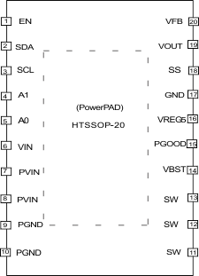
TPS56520/720/920
20-Pin PWP Package with PowerPAD
(TOP VIEW)

Pin Functions
| PIN | I/O | DESCRIPTION | |
|---|---|---|---|
| NAME | NUMBER | ||
| EN | 1 | I | Enable. Pull High to enable converter. |
| SDA | 2 | I/O | Data I/O terminal. |
| SCL | 3 | I/O | Clock I/O terminal. |
| A1, A0 | 4,5 | I | Chip address. |
| VIN | 6 | I | Supply Input for 5.5V linear regulator. |
| PVIN | 7,8 | I | Power inputs and connects to high side MOSFET drains. |
| PGND | 9,10 | I/O | Ground returns for low-side MOSFETs. Input of current comparator. |
| SW | 11,12,13 | I/O | Switch node connections for both the high-side NFETs and low-side NFETs. Input of current comparator. |
| VBST | 14 | I | Supply input for high-side NFET gate drive circuit. Connect 0.1µF ceramic capacitor between VBST and SW terminals. An internal diode is connected between VREG5 and VBST. |
| PGOOD | 15 | O | Open drain power good output. Low means the output voltage of the corresponding output is out of regulation. |
| VREG5 | 16 | O | Output of 5.5V linear regulator. Bypass to GND with a high-quality ceramic capacitor of at least 2.0µF ceramic capacitor. Do not connect any other circuitry to the terminal. VREG5 is active when EN is H-level. |
| GND | 17 | I/O | Signal GND. Connect sensitive SS and VFB returns to GND at a single point. |
| SS | 18 | O | Soft-Start Programming terminal. Connect Capacitor from SS terminal to GND to program Soft-Start time. |
| VOUT | 19 | I | Connection to output voltage |
| VFB | 20 | I | D-CAP2 feedback input. Connect to output voltage with resistor divider. |
| Exposed Thermal Pad | Back side | I/O | Thermal pad of the package. Must be soldered to achieve appropriate dissipation. Must be connected to GND. |
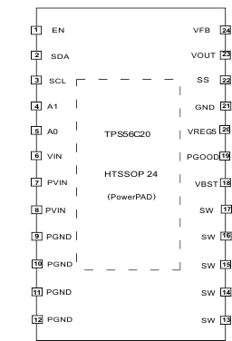
TPS56C20
24-Pin PWP Package with PowerPAD
(TOP VIEW)

Pin Functions
| PIN | I/O | DESCRIPTION | |
|---|---|---|---|
| NAME | NUMBER | ||
| EN | 1 | I | Enable. Pull High to enable according converter. |
| SDA | 2 | I/O | Data I/O terminal. |
| SCL | 3 | I/O | Clock I/O terminal. |
| A1, A0 | 4,5 | I | Chip address. |
| VIN | 6 | I | Supply Input for 5.5V linear regulator. |
| PVIN | 7,8 | I | Power inputs and connects to both high side NFET drains. |
| PGND | 9,10,11,12 | I/O | Ground returns for low-side MOSFETs. Input of current comparator. |
| SW | 13,14,15, 16, 17 | I/O | Switch node connections for both the high-side NFETs and low-side NFETs. Input of current comparator. |
| VBST | 18 | I | Supply input for high-side NFET gate drive circuit. Connect 0.1µF ceramic capacitor between VBST and SW terminals. An internal diode is connected between VREG5 and VBST. |
| PGOOD | 19 | O | Open drain power good output. Low means the output voltage of the corresponding output is out of regulation. |
| VREG5 | 20 | O | Output of 5.5V linear regulator. Bypass to GND with a high-quality ceramic capacitor of at least 3.0µF ceramic capacitor. Do not connect any other circuitry to the terminal. VREG5 is active when EN is H-level. |
| GND | 21 | I/O | Signal GND. Connect sensitive SS and VFB returns to GND at a single point. |
| SS | 22 | O | Soft-Start Programming terminal. Connect Capacitor from SS terminal to GND to program Soft-Start time. |
| VOUT | 23 | I | Connection to output voltage |
| VFB | 24 | I | D-CAP2 feedback inputs. Connect to output voltage with resistor divider. |
| Exposed Thermal Pad | Back side | I/O | Thermal pad of the package. Must be soldered to achieve appropriate dissipation. Must be connected to GND. |