SLVSD05G March 2016 – August 2024 TPS56C215
PRODUCTION DATA
- 1
- 1 Features
- 2 Applications
- 3 Description
- 4 Pin Configuration and Functions
- 5 Specifications
-
6 Detailed Description
- 6.1 Overview
- 6.2 Functional Block Diagram
- 6.3
Feature Description
- 6.3.1 PWM Operation and D-CAP3™ Control Mode
- 6.3.2 Eco-mode Control
- 6.3.3 4.7-V LDO
- 6.3.4 MODE Selection
- 6.3.5 Soft Start and Prebiased Soft Start
- 6.3.6 Enable and Adjustable UVLO
- 6.3.7 Power Good
- 6.3.8 Overcurrent Protection and Undervoltage Protection
- 6.3.9 UVLO Protection
- 6.3.10 Thermal Shutdown
- 6.3.11 Output Voltage Discharge
- 6.4 Device Functional Modes
- 7 Application and Implementation
- 8 Device and Documentation Support
- 9 Revision History
- 10Mechanical, Packaging, and Orderable Information
Package Options
Mechanical Data (Package|Pins)
- RNN|18
Thermal pad, mechanical data (Package|Pins)
Orderable Information
4 Pin Configuration and Functions
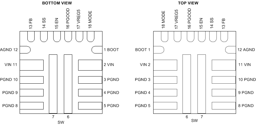
 Figure 4-1 RNN Package,18-Pin VQFN
Table 4-1 Pin Functions
| PIN | TYPE(1) | DESCRIPTION | |
|---|---|---|---|
| NAME | NO. | ||
| BOOT | 1 | I | Supply input for the gate drive voltage of the high-side MOSFET. Connect the bootstrap capacitor between BOOT and SW. |
| VIN | 2,11 | P | Input voltage supply pin for the control circuitry. Connect the input decoupling capacitors between VIN and PGND. |
| PGND | 3, 4, 5, 8, 9, 10 | G | Power GND terminal for the controller circuit and the internal circuitry. Connect to AGND with a short trace. |
| SW | 6, 7 | O | Switch node terminal. Connect the output inductor to this pin. |
| AGND | 12 | G | Ground of internal analog circuitry. Connect AGND to PGND plane with a short trace. |
| FB | 13 | I | Converter feedback input. Connect to the center tap of the resistor divider between output voltage and AGND. |
| SS | 14 | O | Soft-Start time selection pin. Connecting an external capacitor sets the soft-start time and if no external capacitor is connected, the converter starts up in 1 ms. |
| EN | 15 | I | Enable input control, leaving this pin floating enables the converter. It can also be used to adjust the input UVLO by connecting to the center tap of the resistor divider between VIN and EN. |
| PGOOD | 16 | O | Open-drain power good indicator, it is asserted low if output voltage is out of PGOOD threshold, overvoltage, or if the device is under thermal shutdown, EN shutdown or during soft start. |
| VREG5 | 17 | I/O | 4.7-V internal LDO output which can also be driven externally with a 5-V input. This pin supplies voltage to the internal circuitry and gate driver. Bypass this pin with a 4.7-µF capacitor. |
| MODE | 18 | I | Switching frequency, current limit selection and light load operation mode selection pin. Connect this pin to a resistor divider from VREG5 and AGND for different MODE options shown in Table 6-3. |
(1) I = input, P = power, G = ground, O = output