SLUS525A March 2007 – September 2015 TPS61050 , TPS61052
PRODUCTION DATA.
- 1 Features
- 2 Applications
- 3 Description
- 4 Revision History
- 5 Pin Configuration and Functions
- 6 Specifications
- 7 Detailed Description
-
8 Application and Implementation
- 8.1 Application Information
- 8.2
Typical Applications
- 8.2.1 Typical Application Schematic
- 8.2.2 High-Power White LED Solution Featuring Privacy Indicator
- 8.2.3 High-Power White LED Solution Featuring No-Latency Turn-Down Through PA TX Signal
- 8.2.4 High-Power White LED Flash Driver And AF/Zoom Motor Drive Supply
- 8.2.5 White LED Flash Driver and Audio Amplifier Power Supply Exclusive Operation
- 8.2.6 White LED Flash Driver and Audio Amplifier Power Supply Operating Simultaneously
- 8.2.7 White LED Flash Driver and Auxiliary Lighting Zone Power Supply
- 8.2.8 2 × 300 mA Dual LED Camera Flash
- 9 Power Supply Recommendations
- 10Layout
- 11Device and Documentation Support
- 12Mechanical, Packaging, and Orderable Information
Package Options
Mechanical Data (Package|Pins)
Thermal pad, mechanical data (Package|Pins)
- DRC|10
Orderable Information
7 Detailed Description
7.1 Overview
The TPS6105x family employs a 2-MHz constant-frequency, current-mode PWM converter to generate the output voltage required to drive high-power LEDs. The device integrates a power stage based on an NMOS switch and a synchronous NMOS rectifier. The device also implements a linear low-side current regulator to control the LED current when the battery voltage is higher than the diode forward voltage.
In boost mode, the duty cycle of the converter is set by the error amplifier and the saw-tooth ramp applied to the comparator. Because the control architecture is based on a current-mode control, a compensation ramp is added to allow stable operation at duty cycles larger than 50%. The converter is a fully-integrated synchronous-boost converter, always operating in continuous-conduction mode. This allows low-noise operation, and avoids ringing on the switch pin, which would be seen on a converter when entering discontinuous-conduction mode.
The TPS6105x device not only operates as a regulated current source but also as a standard voltage-boost regulator. In the TPS61052 device, the voltage-mode operation can be activated either by a software command or by means of a hardware signal (ENVM). This additional operating mode can be useful to properly synchronize the converter when supplying other high-power devices in the system, such as a hands-free audio power amplifier, or any other component requiring a supply voltage higher than the battery voltage.
The TPS6105x integrates an I2C-compatible interface, allowing transfers up to 400 kbps. This communication interface can be used to
- set the operating mode (shutdown, constant output current mode vs. constant output voltage mode).
- control the brightness of the external LED (torch and flash modes).
- adjust the output voltage (4.5 V / 5 V / 5.25 V) or to program the safety timer.
The torch and flash functions can be controlled by the I2C interface. To simplify flash synchronization with the camera module, the device offers a FLASH_SYNC strobe input pin to switch (with zero latency) the LED current from flash to torch light. The maximum duration of the flash pulse can be limited by means of an internal user-programmable safety timer (STIM).
7.2 Functional Block Diagram
 Figure 15. Functional Block Diagram
 Figure 16. Timer Block Diagram (TPS61050)
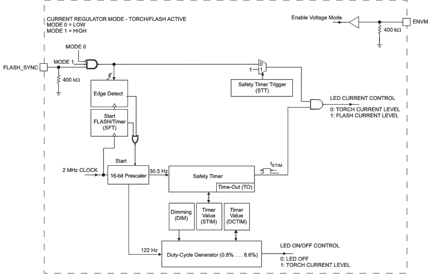 Figure 17. Timer Block Diagram (TPS61052)
7.3 Feature Description
7.3.1 Efficiency
The sense voltage has a direct effect on the converter’s efficiency. Because the voltage across the low-side current regulator does not contribute to the output power (LED brightness), the lower the sense voltage, the higher the efficiency will be.
When running in boost mode (VF(LED) > VIN), the voltage present at the LED pin of the low-side current regulator is typically 250 mV, which contributes to high power-conversion efficiency.
When running in the linear down-converter mode (VF(LED) < VIN), the low-side current regulator drops the voltage difference between the input voltage and the LED forward voltage. Depending on the input voltage and the LED forward voltage characteristic, the converter displays efficiency of approximately 80% to 90%.
7.3.2 Soft-Start
Because the output capacitor always remains biased to the input voltage, the TPS6105x can immediately start switching once it has been enabled through the I2C-compatible interface (refer to MODE_CTRL[1:0] bits). The device starts-up by smoothly ramping up its internal reference voltage, thus limiting the inrush current.
7.3.3 Shutdown
The MODE_CTRL[1:0] bits are low, the device is forced into shutdown. Depending on the setting of OV[1:0] the device can enter different shutdown modes. In shutdown mode, the regulator stops switching and the LED pin is high impedance thus eliminating any DC conduction path.
If OV[1:0] ≠ 11, the internal switch and rectifier MOSFET are turned off. VOUT is one body-diode drop below the input voltage and the device consumes only a shutdown current of 0.3 μA (typical). The output capacitor remains biased to the input voltage.
If OV[1:0] = 11, the internal switch MOSFET is turned off and the rectifier MOSFET is turned on. In this shutdown mode there is almost no dropout voltage between the converter’s input and output. The shutdown current is 150 μA (typical).
7.3.4 LED Failure Modes
If the LED fails as a short circuit, the low-side current regulator limits the maximum output current and the LED FAILURE (LF) flag will be set.
If the LED fails as an open circuit, the control loop initially attempts to regulate off of its low-side current regulator feedback signal. This drives VOUT higher. Because the open-circuited LED will never accept its programmed current, VOUT must be voltage-limited by means of a secondary control loop. In this failure mode, the TPS6105x limits VOUT to 6 V (typical) and sets the LED FAILURE (LF) flag.
7.3.5 Undervoltage Lockout
The undervoltage lockout circuit prevents the device from misoperation at low input voltages. It prevents the converter from turning on the switch or rectifier MOSFET under undefined conditions.
7.3.6 Thermal Shutdown
As soon as the junction temperature, TJ, exceeds 160°C typical, the device goes into thermal shutdown. In this mode, the boost power stage and the low-side current regulator are turned off, the MODE_CTRL[1:0] bits are reset, the OVERTEMP bit is set and can only be reset by a readout.
7.4 Device Functional Modes
7.4.1 Operating Modes: Torch and Flash
The device operation is more easily understood by referring to the timer block diagram. Depending on the settings of MODE_CTRL[1:0] bits the device can enter 4 different operating modes:
- MODE_CTRL[1:0] = 00: The device is in shutdown mode.
- MODE_CTRL[1:0] = 01: The device is regulating the LED current to the torch current level (TC bits) regardless of the FLASH_SYNC input and START_FLASH/TIMER (SFT) bit. The safety timer is disabled in this operating mode.
- MODE_CTRL[1:0] = 11: The device is regulating a constant output voltage according to OV[1:0] bits settings. The low-side LED current regulator is disabled and the LED is disconnected from the output. In this operating mode, the safety timer is disabled and the general purpose timer (DCTIM) can be used to generate a software time-out (TO) flag. DCTIM start is triggered on the rising edge of START_FLASH/TIMER (SFT).
- MODE_CTRL[1:0] = 10: The flash pulse can be either trigger by a hardware signal (FLASH_SYNC) or by a software bit (SFT).
Flash strobe is level sensitive (STT = 0): LED strobe pulse follows FLASH_SYNC
- FLASH_SYNC and (SFT) = 0: LED operation is set to the torch current level and the safety timer is disabled.
- FLASH_SYNC or (SFT) = 1: The LED is driven at the flash current level and the safety timer is running.
The maximum duration of the flash pulse is defined in the STIM register.
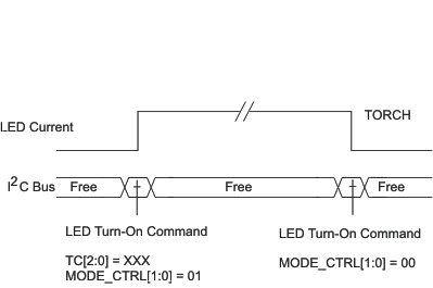 Figure 18. Torch Mode Operation
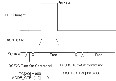 Figure 19. Synchronized Flash Strobe
 Figure 20. Level Sensitive Safety Timer (Time-Out)
 Figure 21. Level Sensitive Safety Timer (Normal Operation + Time-Out)
The safety timer is started by:
- a rising edge of FLASH_SYNC signal.
- a rising edge of START_FLASH/TIMER (SFT) bit.
The safety timer is stopped by:
- a low level of FLASH_SYNC signal or START_FLASH/TIMER (SFT) bit.
- a time-out signal (TO).
The START-FLASH/TIMER (SFT) bit is reset by the time-out (TO) signal.
The Flash strobe is edge sensitive (STT = 1): The LED strobe pulse is triggered by a rising edge
When FLASH_SYNC and START_FLASH/TIMER (SFT) are both low, the LED operation is set to the torch current level without time-out.
The duration of the flash pulse is defined in the STIM register. The flash strobe is started by:
- a rising edge of FLASH_SYNC signal.
- a rising edge of START_FLASH/TIMER (SFT) bit.
Once running, the timer ignores any triggering signal, and only stops after a time-out (TO). The START-FLASH/TIMER (SFT) bit is reset by the time-out (TO) signal.
 Figure 22. Edge Sensitive Timer (Single Trigger Event)
 Figure 23. Edge Sensitive Timer (Single Trigger Event)
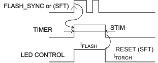 Figure 24. Edge Sensitive Timer (Multiple Trigger Events)
7.4.2 Mode of Operation: Flash Blanking (TPS61050)
The TPS61050 device also integrates a general purpose I/O pin (GPIO) that can be configured either as a standard logic input/output or as a flash masking input (Tx-MASK). This blanking function turns the LED from flash to torch light, thereby reducing almost instantaneously the peak current loading from the battery. The Tx-MASK function has no influence on the safety timer duration.
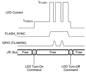 Figure 25. Synchronized Flash With Blanking Periods
7.4.3 Hardware Voltage Mode Selection (TPS61052)
The TPS61052 device integrates a logic input (ENVM) that can be used to force the converter to run in voltage mode regulation. This additional operating mode can be useful to supply other high power consumption devices in the system (for example, hands-free audio power amplifier) or any other component requiring a supply voltage higher than the battery voltage.
Table 2 gives an overview of the different mode of operation of TPS61052.
Table 2. TPS61052 Operating Modes
| INTERNAL REGISTER SETTINGS MODE_CTRL[1:0] | ENVM | OPERATING MODES |
|---|---|---|
| 00 | 0 | Power stage is in shutdown. The output is either connected directly to the battery (OV[1:0]=11, rectifier is bypassed) or through the rectifer’s body diode (OV[1:0]=01). In both case the power stage LC filter is connected in series between the battery and the output. |
| 01 | 0 | LED is turned-on for DC light operation. The converter is operating in the current regulation mode (CM). The output voltage is controlled by the forward voltage characteristic of the LED. |
| 10 | 0 | LED is turned-on for flash operation. The converter is operating in the current regulation mode (CM). The output voltage is controlled by the forward voltage characteristic of the LED. |
| 11 | 0 | LED is turned-off and the converter is operating in the voltage regulation mode (VM). The output voltage is set through the register OV[1:0]. |
| 00 | 1 | LED is turned-off and the converter is operating in the voltage regulation mode (VM). The output voltage is set through the register OV[1:0]. |
| 01 | 1 | The converter is operating in the voltage regulation mode (VM) and it’s output voltage is set through the register OV[1:0]. The LED is turned-on for torch operation according to the register TC[2:0]. The LED current is regulated by the means of the low-side current sink. |
| 10 | 1 | The converter is operating in the voltage regulation mode (VM) and it’s output voltage is set through the register OV[1:0]. The LED is turned-on for flash operation according to the register FC[2:0]. The LED current is regulated by the means of the low-side current sink. |
| 11 | 1 | LED is turned-off and the converter is operating in the voltage regulation mode (VM). The output voltage is set through the register OV[1:0]. |
7.4.4 Low Light Dimming Mode
The TPS6105x device features white LED drive capability at very low light intensity. To generate a reduced LED average current, the device employs a 122-Hz fixed frequency PWM modulation scheme. Operation is understood best by referring to the timer block diagram.
The torch current is modulated with a duty cycle defined by the DCTIM[2:0] bits. The low light dimming mode can only be activated in the torch only mode, MODE_CTRL[1:0] = 01.
 Figure 26. PWM Dimming Principle
White LED blinking can be achieved by turning on/off periodically the LED dimmer through the (DIM) bit, see Figure 27.
 Figure 27. White LED Blinking Control
7.5 Programming
7.5.1 3-Bit ADC
The TPS6105x device integrates a 3 bit A/D converter to measure the differential voltage across the output and the low-side current regulator. To get a proper settling of the LED forward voltage, the data acquisition is done approximately 10 ms after the start of the flash sequence.
When running in the linear down-mode (VF(LED) < VIN), the low-side current regulator drops the voltage difference between the input voltage and the LED forward voltage. This may result in thermal limitations (especially for CSP-12 packaging) when running high LED current under high battery conditions (VIN ≥ 4.5 V) with low forward voltage LEDs and/or high ambient temperature.
The LED forward voltage measurement can be started either by a START FLASH event (FLASH_SYNC or SFT bit) or by setting ADC[2:0] bits (whilst MODE_CTRL[1:0]=01 or 10).
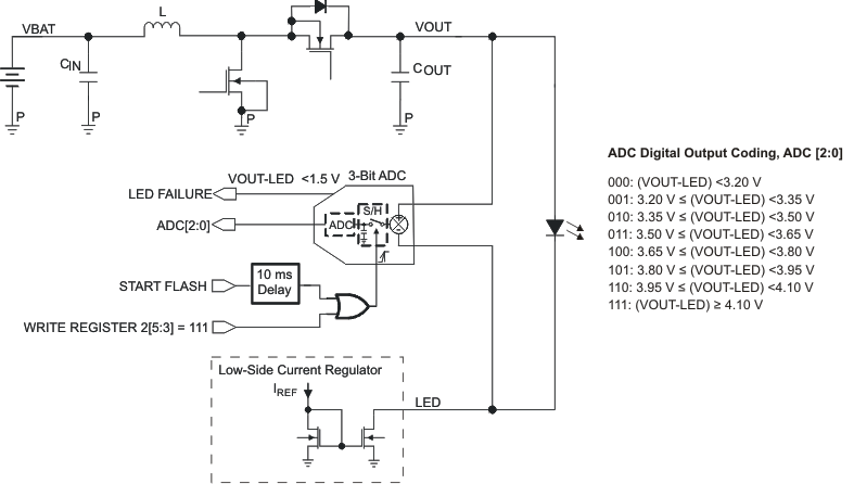 Figure 28. LED VF Measurement Principle
7.5.2 Serial Interface Description
I2C is a 2-wire serial interface developed by Philips Semiconductor (see I2C-Bus Specification, Version 2.1, January 2000). The bus consists of a data line (SDA) and a clock line (SCL) with pullup structures. When the bus is idle, both SDA and SCL lines are pulled high. All the I2C compatible devices connect to the I2C bus through open-drain I/O pins, SDA and SCL. A master device, usually a microcontroller or a digital signal processor, controls the bus. The master is responsible for generating the SCL signal and device addresses. The master also generates specific conditions that indicate the START and STOP of data transfer. A slave device receives and/or transmits data on the bus under control of the master device.
The TPS6105x device works as a slave and supports the following data transfer modes, as defined in the I2C-Bus Specification: standard mode (100 kbps) and fast mode (400 kbps). The interface adds flexibility to the power supply solution, enabling most functions to be programmed to new values depending on the instantaneous application requirements. Register contents remain intact as long as the supply voltage remains greater than approximately 2 V.
The data transfer protocol for standard and fast modes is exactly the same, therefore they are referred to as F/S-mode in this document. The TPS6105x device supports 7-bit addressing; 10-bit addressing and general call address are not supported. The device 7-bit address is defined as 011 0011.
7.5.3 F/S-Mode Protocol
The master initiates data transfer by generating a start condition. The start condition is when a high-to-low transition occurs on the SDA line while SCL is high, as shown in Figure 29 All I2C-compatible devices should recognize a start condition.
 Figure 29. Start and Stop Conditions
The master then generates the SCL pulses, and transmits the 7-bit address and the read/write direction bit R/W on the SDA line. During all transmissions, the master ensures that data is valid. A valid data condition requires the SDA line to be stable during the entire high period of the clock pulse (see Figure 30). All devices recognize the address sent by the master and compare it to their internal fixed addresses. Only the slave device with a matching address generates an acknowledge (see Figure 31) by pulling the SDA line low during the entire high period of the ninth SCL cycle. Upon detecting this acknowledge, the master knows that communication link with a slave has been established.
 Figure 30. Bit Transfer on the Serial Interface
The master generates further SCL cycles to either transmit data to the slave (R/W bit 1) or receive data from the slave (R/W bit 0). In either case, the receiver must acknowledge the data sent by the transmitter. So an acknowledge signal can either be generated by the master or by the slave, depending on which one is the receiver. 9-bit valid data sequences consisting of 8-bit data and 1-bit acknowledge can continue as long as necessary.
To signal the end of the data transfer, the master generates a stop condition by pulling the SDA line from low to high while the SCL line is high (see Figure 29). This releases the bus and stops the communication link with the addressed slave. All I2C compatible devices must recognize the stop condition. Upon the receipt of a stop condition, all devices know that the bus is released, and they wait for a start condition followed by a matching address.
Attempting to read data from register addresses not listed in this section will result in 00h being read out.
 Figure 31. Acknowledge on the I2C Bus
 Figure 32. Bus Protocol
7.5.4 TPS6105X I2C Update Sequence
The TPS6105x requires a start condition, a valid I2C address, a register address byte, and a data byte for a single update. After the receipt of each byte, TPS6105x device acknowledges by pulling the SDA line low during the high period of a single clock pulse. A valid I2C address selects the TPS6105x. TPS6105x performs an update on the rising edge of the SCL clock that follows the ACK bit transmission.
 Figure 33. Write Data Transfer Format In F/S-Mode
 Figure 34. Read Data Transfer Format In F/S-Mode
| SLAVE ADDRESS BYTE |
| MSB | LSB | ||||||
| X | 0 | 1 | 1 | 0 | 0 | 1 | 1 |
The slave address byte is the first byte received following the START condition from the master device.
| REGISTER ADDRESS BYTE |
| MSB | LSB | ||||||
| 0 | 0 | 0 | 0 | 0 | 0 | D1 | D0 |
Following the successful acknowledgement of the slave address, the bus master will send a byte to the TPS6105x, which will contain the address of the register to be accessed. The TPS6105x contains four 8-bit registers accessible through a bidirectional I2C-bus interface. All internal registers have read and write access.
7.6 Register Maps
7.6.1 Register Description

 Figure 36. Register1 (Read/Write) (TPS6105X)
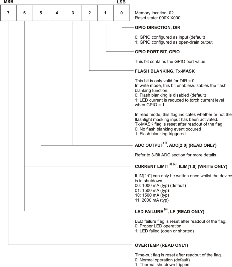
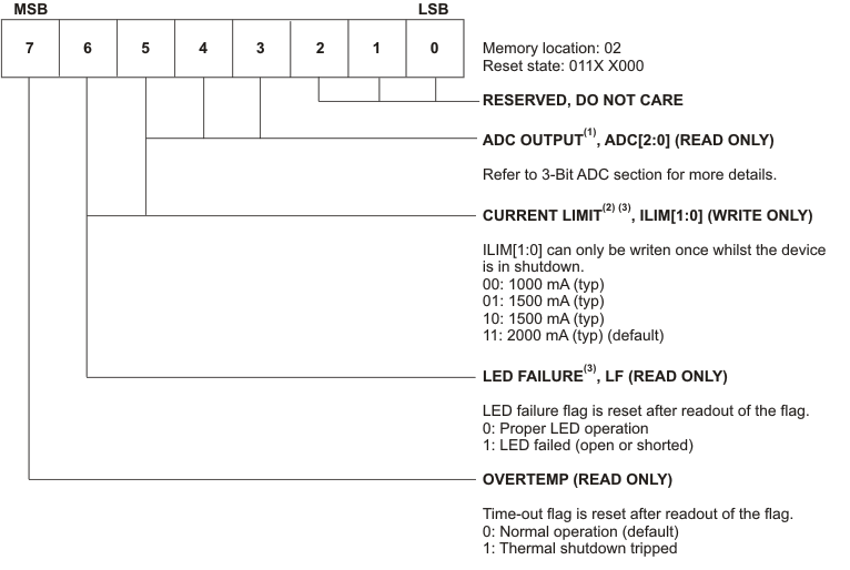
 Figure 39. Register3 (Read/Write) (TPS6105X)