SLVS431C june   2002  – September 2015 TPS61130 , TPS61131

PRODUCTION DATA.  

  1. Features
  2. Applications
  3. Description
  4. Revision History
  5. Available Output Voltage Options
  6. Pin Configuration and Functions
  7. Specifications
    1. 7.1 Absolute Maximum Ratings
    2. 7.2 ESD Ratings
    3. 7.3 Recommended Operating Conditions
    4. 7.4 Thermal Information
    5. 7.5 Electrical Characteristics
    6. 7.6 Typical Characteristics
  8. Parameter Measurement Information
  9. Detailed Description
    1. 9.1 Overview
    2. 9.2 Functional Block Diagram
    3. 9.3 Feature Description
      1. 9.3.1 Controller Circuit
      2. 9.3.2 Synchronous Rectifier
      3. 9.3.3 Device Enable
      4. 9.3.4 Undervoltage Lockout
      5. 9.3.5 Soft-Start
      6. 9.3.6 Power Good
      7. 9.3.7 Low Battery Detector Circuit—LBI/LBO
      8. 9.3.8 Low-EMI Switch
    4. 9.4 Device Functional Modes
      1. 9.4.1 Power Save Mode
      2. 9.4.2 LDO
      3. 9.4.3 LDO Enable
  10. 10Application and Implementation
    1. 10.1 Application Information
    2. 10.2 Typical Applications
      1. 10.2.1 Typical Application Circuit for Adjustable Output Voltage Option
        1. 10.2.1.1 Design Requirements
        2. 10.2.1.2 Detailed Design Procedure
          1. 10.2.1.2.1 Programming the Output Voltage
            1. 10.2.1.2.1.1 DC-DC Converter
          2. 10.2.1.2.2 LDO
          3. 10.2.1.2.3 Programming the LBI/LBO Threshold Voltage
          4. 10.2.1.2.4 Inductor Selection
          5. 10.2.1.2.5 Capacitor Selection
            1. 10.2.1.2.5.1 Input Capacitor
            2. 10.2.1.2.5.2 Flying Capacitor DC-DC Converter
            3. 10.2.1.2.5.3 Output Capacitor DC-DC Converter
            4. 10.2.1.2.5.4 Small Signal Stability
            5. 10.2.1.2.5.5 Output Capacitor LDO
        3. 10.2.1.3 Application Curves
      2. 10.2.2 Solution for Maximum Output Power
      3. 10.2.3 Low Profile Solution, Maximum Height 1.8 mm
      4. 10.2.4 Single Output Using LDO as Filter
      5. 10.2.5 Dual Input Power Supply Solution
  11. 11Power Supply Recommendations
  12. 12Layout
    1. 12.1 Layout Guidelines
    2. 12.2 Layout Example
    3. 12.3 Thermal Consideration
  13. 13Device and Documentation Support
    1. 13.1 Device Support
      1. 13.1.1 Third-Party Products Disclaimer
    2. 13.2 Related Links
    3. 13.3 Community Resource
    4. 13.4 Trademarks
    5. 13.5 Electrostatic Discharge Caution
    6. 13.6 Glossary
  14. 14Mechanical, Packaging, and Orderable Information

Package Options

Mechanical Data (Package|Pins)
Thermal pad, mechanical data (Package|Pins)
Orderable Information

8 Parameter Measurement Information
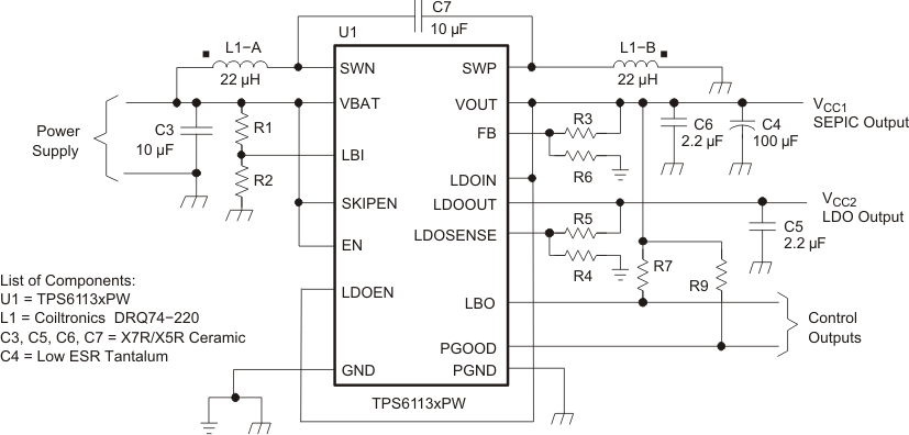
TPS61130 TPS61131 TPS61132 pmi_circuit_LVS431.gif