SLVSBR3A May 2013 – June 2015 TPS61158
PRODUCTION DATA.
- 1 Features
- 2 Applications
- 3 Description
- 4 Revision History
- 5 Pin Configuration and Functions
- 6 Specifications
- 7 Detailed Description
- 8 Application and Implementation
- 9 Power Supply Recommendations
- 10Layout
- 11Device and Documentation Support
- 12Mechanical, Packaging, and Orderable Information
Package Options
Mechanical Data (Package|Pins)
- DRV|6
Thermal pad, mechanical data (Package|Pins)
- DRV|6
Orderable Information
10 Layout
10.1 Layout Guidelines
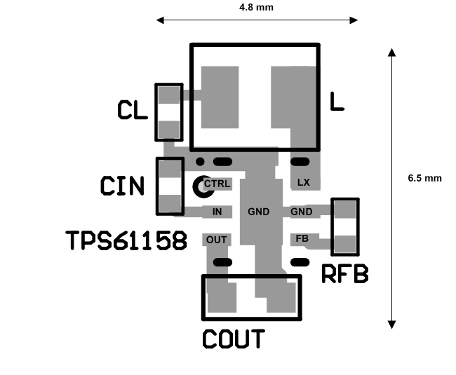
As for all switching power supplies, especially those high frequency and high current ones, layout is an important design step. If layout is not carefully done, the regulator could suffer from instability as well as noise problems. Therefore, use wide and short traces for high current paths. The input capacitor CIN needs to be close to the VIN pin and GND pin in order to reduce the input ripple seen by the device. If possible, choose higher capacitance value for it. If the ripple seen at VIN pin is so large that it affects the boost loop stability or internal circuits operation, R1 and C1 is recommended to compose a filter to decouple the noise (refer to Figure 24). The SW pin carries high current with fast rising and falling edges. Therefore, the connection between the SW pin to the inductor should be kept as short and wide as possible. The output capacitor COUT should be put close to VOUT pin. It is also beneficial to have the ground of COUT close to the GND pin since there is large ground return current flowing between them. FB resistor should be put close to FB pin. When laying out signal grounds, it is recommended to use short traces separated from power ground traces, and connect them together at a single point close to the GND pin.
10.2 Layout Example
 Figure 25. TPS61158 Example Layout