SLVSBG1D October 2012 – May 2015 TPS61196
PRODUCTION DATA.
- 1 Features
- 2 Applications
- 3 Description
- 4 Revision History
- 5 Pin Configuration and Functions
- 6 Specifications
-
7 Detailed Description
- 7.1 Overview
- 7.2 Functional Block Diagram
- 7.3 Feature Description
- 7.4
Device Functional Modes
- 7.4.1
Protections
- 7.4.1.1 Switch Current Limit Protection Using the ISNS Pin
- 7.4.1.2 LED Open Protection
- 7.4.1.3 LED Short-Cross Protection Using the FBP Pin
- 7.4.1.4 Schottky Diode Open Protection
- 7.4.1.5 Schottky Diode Short Protection
- 7.4.1.6 IFB Overvoltage Protection During Start-up
- 7.4.1.7 Output Overvoltage Protection Using the OVP Pin
- 7.4.1.8 Output Short-to-Ground Protection
- 7.4.1.9 IFB Short-to-Ground Protection
- 7.4.1.10 ISET Short-to-Ground Protection
- 7.4.1.11 Thermal Protection
- 7.4.2 Indication For Fault Conditions
- 7.4.1
Protections
- 8 Application and Implementation
- 9 Power Supply Recommendations
- 10Layout
- 11Device and Documentation Support
- 12Mechanical, Packaging, and Orderable Information
Package Options
Mechanical Data (Package|Pins)
- PWP|28
Thermal pad, mechanical data (Package|Pins)
- PWP|28
Orderable Information
5 Pin Configuration and Functions
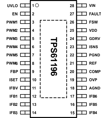
PWP Package
28-Pin HTSSOP
Top View

Pin Functions
| PIN | TYPE | DESCRIPTION | |
|---|---|---|---|
| NUMBER | NAME | ||
| 1 | UVLO | I | Low input voltage lockout. Use a resistor divider from VIN to this pin to set the UVLO threshold. |
| 2 | EN | I | Enable and disable pin. EN high = enable, EN low = disable. |
| 3,4,5,6,7,8 | PWM1 to PWM6 | I | PWM signal input pins. The frequency of PWM signal is in the range of 90 Hz to 22 kHz. |
| 9 | FBP | O | LED cross-short protection threshold program pin. Use a resistor to GND to set the threshold. |
| 10 | ISET | O | Connecting a resistor to the pin programs the IFB pin current level for full brightness (that is, 100% dimming). |
| 11 | IFBV | O | Minimum feedback voltage setting for LED strings. |
| 12,13,14,15,16,17 | IFB1 to IFB6 | I | Regulated current sink input pins |
| 18 | AGND | G | Analog ground |
| 19 | OVP | I | Overvoltage protection detection input. Connect a resistor divider from output to this pin to program the OVP threshold. |
| 20 | COMP | O | Loop compensation for the boost converter. Connect a RC network to make loop stable. |
| 21 | REF | O | Internal reference voltage for the boost converter. Use a capacitor at this pin to adjust the soft start time. When two chips operate in parallel, connect the master's REF pin to the slave's COMP pin. |
| 22 | PGND | G | External MOSFET current sense ground input. |
| 23 | ISNS | I | External MOSFET current sense positive input. |
| 24 | GDRV | o | External switch MOSFET gate driver output. |
| 25 | VDD | O | Internal regulator output for device internal power supply. Connect a 1-µF ceramic capacitor to this pin. |
| 26 | FSW | O | Switching frequency setting pin. Use a resistor to set the frequency between 100 kHz to 800 kHz. An external input voltage above 3.5 V or below 0.5 V disables the internal clock and makes the device as slave device. |
| 27 | FAULT | O | Fault indicator. Open-drain output. Output high impedance when fault conditions happens. |
| 28 | VIN | I | Power supply input pin |