TPS6120x Low Input Voltage Synchronous Boost Converter With 1.3-A Switches
1 Features
- More than 90% Efficiency at
- Automatic Transition between Boost Mode and Down Conversion Mode
- Device Quiescent Current Less than 55 μA
- Startup into Full Load at 0.5 V Input Voltage
- Operating Input Voltage Range from
0.3 V to 5.5 V - Programmable Undervoltage Lockout Threshold
- Output Short Circuit Protection Under all Operating Conditions
- Fixed and Adjustable Output Voltage Options from 1.8 V to 5.5 V
- Power Save Mode for Improved Efficiency at Low Output Power
- Forced Fixed Frequency Operation Possible
- Load Disconnect During Shutdown
- Overtemperature Protection
- Small 3 mm x 3 mm VSON-10 Package
2 Applications
3 Description
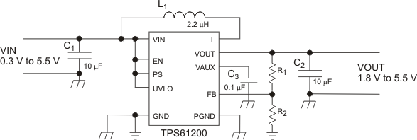
The TPS6120x devices provide a power supply solution for products powered by either a single-cell, two-cell, or three-cell alkaline, NiCd or NiMH, or one-cell Li-Ion or Li-polymer battery. It is also used in fuel cell or solar cell powered devices where the capability of handling low input voltages is essential. Possible output currents depend on the input to output voltage ratio. The devices provide output currents of up to 600 mA at a 5-V output, while using a single-cell Li-Ion or Li-Polymer battery and discharges it down to 2.6 V. The boost converter is based on a fixed frequency, pulse-width-modulation (PWM) controller using synchronous rectification to obtain maximum efficiency. At low load currents, the converter enters the Power Save mode to maintain a high efficiency over a wide load current range. The Power Save mode can be disabled, forcing the converter to operate at a fixed switching frequency. The average input current is limited to a maximum value of 1500 mA. The output voltage is programmed by an external resistor divider, or is fixed internally on the chip. The converter can be disabled to minimize battery drain. During shutdown, the load is completely disconnected from the battery. The device is packaged in a 10-pin VSON package measuring 3 mm x 3 mm.
Device Information(1)
| PART NUMBER | PACKAGE | BODY SIZE (NOM) |
|---|---|---|
| TPS6120x | VSON (10) | 3.00 mm × 3.00 mm |
- For all available packages, see the orderable addendum at the end of the datasheet.
4 Typical Application
5 Revision History
Changes from D Revision (March 2013) to E Revision
- Added ESD Ratings table, Feature Description section, Device Functional Modes, Application and Implementation section, Power Supply Recommendations section, Layout section, Device and Documentation Support section, and Mechanical, Packaging, and Orderable Information sectionGo
Changes from C Revision (September 2012) to D Revision
- Changed the PS pin description From: Enable/disable Power Save mode (High = enabled, Low = disabled) To: Enable/disable Power Save mode (High = disabled, Low = enabled)Go
Changes from B Revision (FEBRUARY 2008) to C Revision
- Changed Feature From: Small 3 mm x 3 mm QFN-10 Package To: Small 3 mm x 3 mm SON-10 PackageGo
- Changed Application From: White LED's To: White LED DriverGo
- Changed the Available Device Options Package type From: 10-PIN QFN To: 10-Pin SONGo
- Changed VSS to VIN in the Recommended Operating Conditions tableGo
- Changed From: DISSIPATION RATINGS TABLE To: Thermal Information table Go
- Changed the Parameters and Test Conditions in the Electrical Characteristics table Go
- Updated Figure 1 through Figure 11Go
- Added C3 to the List of ComponentsGo
- Added text to the Input Capacitor section "An R-C filter may be placed..."Go
- Added Figure 26, Figure 27, and Figure 28Go
- Added Figure 29Go
Changes from A Revision (JUNE 2007) to B Revision
- Added DSC package and tape and reel note to the Available Device Options.Go
Changes from * Revision (MARCH 2007) to A Revision
6 Device Options
| TA | OUTPUT VOLTAGE(1) | PART NUMBER(2) |
|---|---|---|
| –40°C to 85°C | Adjustable | TPS61200DRC |
| 3.3 V | TPS61201DRC | |
| 5 V | TPS61202DRC | |
| 5 V | TPS61202DSC |
7 Pin Configuration and Functions
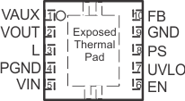
Pin Functions
8 Specifications
8.1 Absolute Maximum Ratings
over operating free-air temperature range (unless otherwise noted)(1)| MIN | MAX | UNIT | ||
|---|---|---|---|---|
| VIN | Input voltage range on VIN, L, VAUX, VOUT, PS, EN, FB, UVLO | –0.3 | 7 | V |
| TJ | Operating junction temperature | –40 | 150 | °C |
| Tstg | Storage temperature | –65 | 150 | °C |
8.2 ESD Ratings
| VALUE | UNIT | |||
|---|---|---|---|---|
| V(ESD) | Electrostatic discharge | Human-body model (HBM), per ANSI/ESDA/JEDEC JS-001(1) | ±4000 | V |
| Charged-device model (CDM), per JEDEC specification JESD22-C101(2) | ±1500 | |||
| Machine Model (MM)(3) | ±200 | |||
8.3 Recommended Operating Conditions
| MIN | NOM | MAX | UNIT | ||
|---|---|---|---|---|---|
| VIN | Input voltage at VIN | 0.3 | 5.5 | V | |
| TA | Operating free air temperature range | –40 | 85 | °C | |
| TJ | Operating junction temperature range | –40 | 125 | °C | |
8.4 Thermal Information
| THERMAL METRIC(1) | TPS6120x | UNIT | ||
|---|---|---|---|---|
| DRC | DSC | |||
| 10 PINS | 10 PINS | |||
| RθJA | Junction-to-ambient thermal resistance | 41.2 | 40.4 | °C/W |
| RθJC(top) | Junction-to-case (top) thermal resistance | 62.8 | 37.8 | |
| RθJB | Junction-to-board thermal resistance | 16.6 | 15.4 | |
| ψJT | Junction-to-top characterization parameter | 1.2 | 0.3 | |
| ψJB | Junction-to-board characterization parameter | 16.8 | 15.6 | |
| RθJC(bot) | Junction-to-case (bottom) thermal resistance | 4.1 | 2.8 | |
8.5 Electrical Characteristics
over recommended junction temperature range and over recommended input voltage range (typical at an ambient temperature range of 25°C) (unless otherwise noted)| PARAMETER | TEST CONDITIONS | MIN | TYP | MAX | UNIT | ||
|---|---|---|---|---|---|---|---|
| DC-DC STAGE | |||||||
| VIN | Input voltage range | 0.3 | 5.5 | V | |||
| VIN | Minimum input voltage at startup | 0.5 | V | ||||
| VOUT | TPS61200 output voltage range | 1.8 | 5.5 | V | |||
| VFB | TPS61200 feedback voltage | 495 | 500 | 505 | mV | ||
| VOUT | TPS61201 output voltage | VIN < VOUT, PS = High | 3.27 | 3.3 | 3.33 | V | |
| VOUT | TPS61202 output voltage | VIN < VOUT, PS = High | 4.95 | 5.0 | 5.05 | V | |
| f | Oscillator frequency | 1250 | 1650 | kHz | |||
| ILIM | average inductor current limit | VOUT = 3.3 V | 1200 | 1350 | 1500 | mA | |
| RDS(on) | Rectifying switch on resistance | VOUT = 3.3 V | 180 | mΩ | |||
| RDS(on) | Main switch on resistance | VOUT = 3.3 V | 150 | mΩ | |||
| Line regulation | VIN < VOUT, PS = High | 0.1% | 0.5% | ||||
| Load regulation | VIN < VOUT, PS = High | 0.1% | 0.5% | ||||
| IQ | Quiescent current | VIN | IO = 0 mA, VEN = VIN = 1.2 V, VOUT = 3.3 V, VAUX = 3.3 V PS = Low |
1 | 2 | μA | |
| VOUT | 50 | 70 | μA | ||||
| VAUX | 4 | 6 | μA | ||||
| ISD | Shutdown current | VIN | VEN = 0 V, VIN = 1.2 V | 0.5 | 1.5 | μA | |
| VAUX | 1 | 2 | μA | ||||
| ILKG | Input leakage current ( L) | VEN = 0 V, VIN = 1.2 V, VL = 1.2 V | 0.01 | 1 | μA | ||
| CONTROL STAGE | |||||||
| VAUX | Auxiliary Output Voltage | 2.4 | 5.5 | V | |||
| VIL | Low level input threshold voltage (EN) | VIN < 0.8 V | 0.1 × VIN | V | |||
| VIH | High level input threshold voltage (EN) | VIN < 0.8 V | 0.9 × VIN | V | |||
| VIL | Low level input threshold voltage (EN) | 0.8 V ≤ VIN ≤ 1.5 V | 0.2 × VIN | V | |||
| VIH | High level input threshold voltage (EN) | 0.8 V ≤ VIN ≤ 1.5 V | 0.8 × VIN | V | |||
| VIL | Low level input threshold voltage (EN) | VIN > 1.5 V | 0.4 | V | |||
| VIH | High level input threshold voltage (EN) | VIN > 1.5 V | 1.2 | V | |||
| VIL | Low level input threshold voltage (PS) | 0.4 | V | ||||
| VIH | High level input threshold voltage (PS) | 1.2 | V | ||||
| ILKG | Input leakage current (EN, PS) | EN, PS = GND or VIN | 0.01 | 0.1 | μA | ||
| VUVLO | Undervoltage lockout threshold | Falling UVLO voltage | 235 | 250 | 265 | mV | |
| VUVLO | Undervoltage lockout threshold | Rising UVLO voltage | 330 | 350 | 370 | mV | |
| ILKG | Input leakage current (UVLO) | VUVLO = 0.5 V | 0.3 | μA | |||
| VOVP | Overvoltage protection threshold | 5.5 | 7 | V | |||
| Thermal shutdown temperature | Rising temperature | 140 | °C | ||||
| Thermal shutdown temperature hysteresis | 20 | °C | |||||
8.6 Typical Characteristics
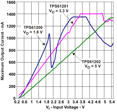
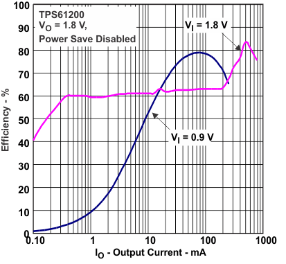
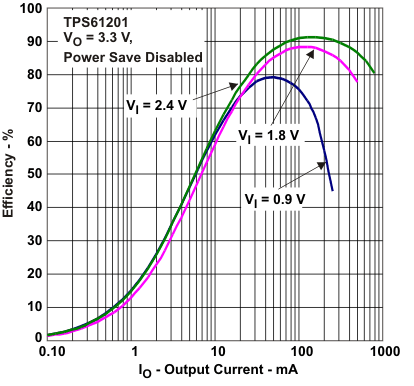
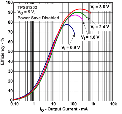
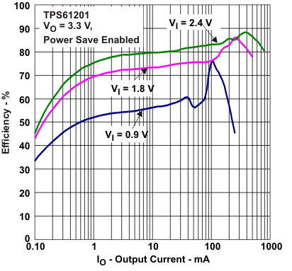
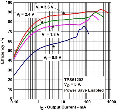
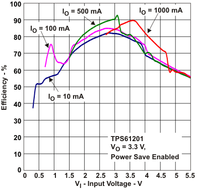
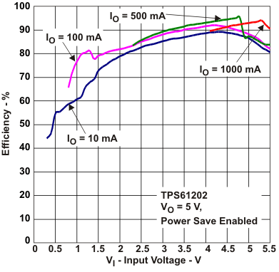
Table 1. Table of Graphs
| FIGURE | |||
|---|---|---|---|
| Maximum output current | vs Input voltage | Figure 1 | |
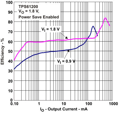
| Efficiency | vs Output current (TPS61200), Power Save Enabled | Figure 2 | |
| vs Output current (TPS61200), Power Save Disabled | Figure 3 | ||
| vs Output current (TPS61201), Power Save Enabled | Figure 4 | ||
| vs Output current (TPS61201), Power Save Disabled | Figure 5 | ||
| vs Output current (TPS61202), Power Save Enabled | Figure 6 | ||
| vs Output current (TPS61202), Power Save Disabled | Figure 7 | ||
| vs Input voltage (TPS61201), Power Save Enabled | Figure 8 | ||
| vs Input voltage (TPS61201), Power Save Disabled | Figure 9 | ||
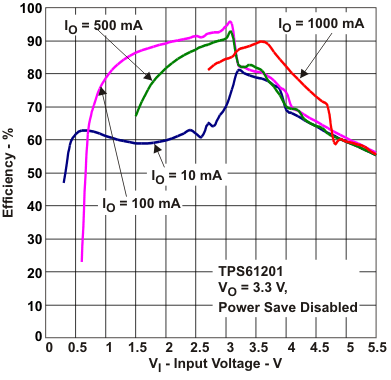
| vs Input voltage (TPS61202), Power Save Enabled | Figure 10 | ||
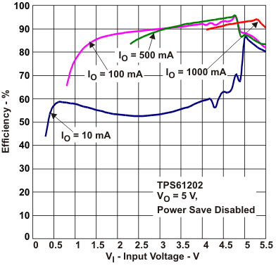
| vs Input voltage (TPS61202), Power Save Disabled | Figure 11 | ||
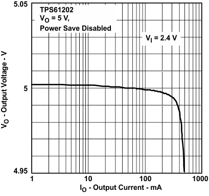
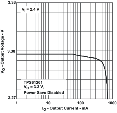
| Output voltage | vs Output current (TPS61201) | Figure 12 | |
| vs Output current (TPS61202) | Figure 13 | ||