SLVSEE7B June 2018 – January 2021 TPS61372
PRODUCTION DATA
- 1 Features
- 2 Applications
- 3 Description
- 4 Revision History
- 5 Pin Configuration and Functions
- 6 Specifications
- 7 Detailed Description
-
8 Application and Implementation
- 8.1 Application Information
- 8.2
Typical Application
- 8.2.1 Design Requirements
- 8.2.2
Detailed Design Procedure
- 8.2.2.1 Custom Design With WEBENCH® Tools
- 8.2.2.2 Setting the Output Voltage
- 8.2.2.3 Selecting the Inductor
- 8.2.2.4 Selecting the Output Capacitors
- 8.2.2.5 Selecting the Input Capacitors
- 8.2.2.6 Loop Stability and Compensation
- 8.2.2.7 Loop Compensation Design Steps
- 8.2.2.8 Selecting the Bootstrap Capacitor
- 8.2.3 Application Curves
- 9 Power Supply Recommendations
- 10Layout
- 11Device and Documentation Support
- 12Mechanical, Packaging, and Orderable Information
Package Options
Refer to the PDF data sheet for device specific package drawings
Mechanical Data (Package|Pins)
- YKB|16
Thermal pad, mechanical data (Package|Pins)
Orderable Information
7.4.2 Auto PFM Mode
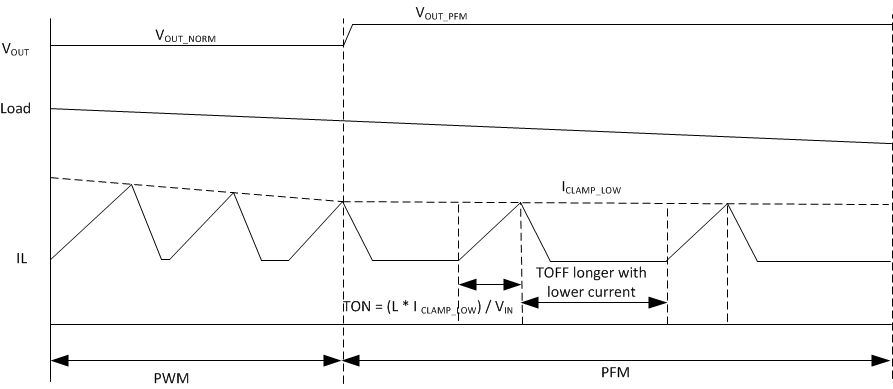
The TPS61372 integrates a power-save mode with pulse frequency modulation (PFM) at light load (set the mode pin low logic or floating). The device skips the switching cycles and regulates the output voltage at a higher threshold (typically 101.6% × VOUT_NORM). Figure 7-1 shows the working principle of the PFM operation. The auto PFM mode reduces the switching losses and improves efficiency at light load condition by reducing the average switching frequency.
 Figure 7-1 Auto PFM Operation Behavior