SLVSET0E May 2020 – October 2024 TPS61378-Q1
PRODUCTION DATA
- 1
- 1 Features
- 2 Applications
- 3 Description
- 4 Device Comparison Table
- 5 Pin Configuration and Functions
- 6 Specifications
-
7 Detailed Description
- 7.1 Overview
- 7.2 Functional Block Diagram
- 7.3
Feature Description
- 7.3.1 VCC Power Supply
- 7.3.2 Input Undervoltage Lockout (UVLO)
- 7.3.3 Enable and Soft Start
- 7.3.4 Shut Down
- 7.3.5 Switching Frequency Setting
- 7.3.6 Spread Spectrum Frequency Modulation
- 7.3.7 Adjustable Peak Current Limit
- 7.3.8 Bootstrap
- 7.3.9 Load Disconnect
- 7.3.10 MODE/SYNC Configuration
- 7.3.11 Overvoltage Protection (OVP)
- 7.3.12 Output Short Protection/Hiccup
- 7.3.13 Power-Good Indicator
- 7.3.14 Thermal Shutdown
- 7.4 Device Functional Modes
-
8 Application and Implementation
- 8.1 Application Information
- 8.2
Typical Application
- 8.2.1 Design Requirements
- 8.2.2 Detailed Design Procedure
- 8.2.3 Application Curves
- 9 Power Supply Recommendations
- 10Layout
- 11Device and Documentation Support
- 12Revision History
- 13Mechanical, Packaging, and Orderable Information
Package Options
Mechanical Data (Package|Pins)
- RTE|16
Thermal pad, mechanical data (Package|Pins)
- RTE|16
Orderable Information
6.6 Typical Characteristics
VIN = 3.3 V, VOUT
= 9 V (VO pin), TA = 25°C, Fsw = 2.2 MHz, unless otherwise
noted.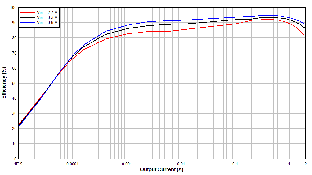
Figure 6-1 5 VOUT
Efficiency vs Output Current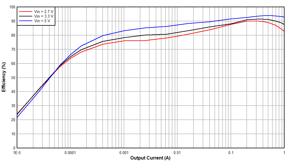
Figure 6-3 9 VOUT
Efficiency vs Output Current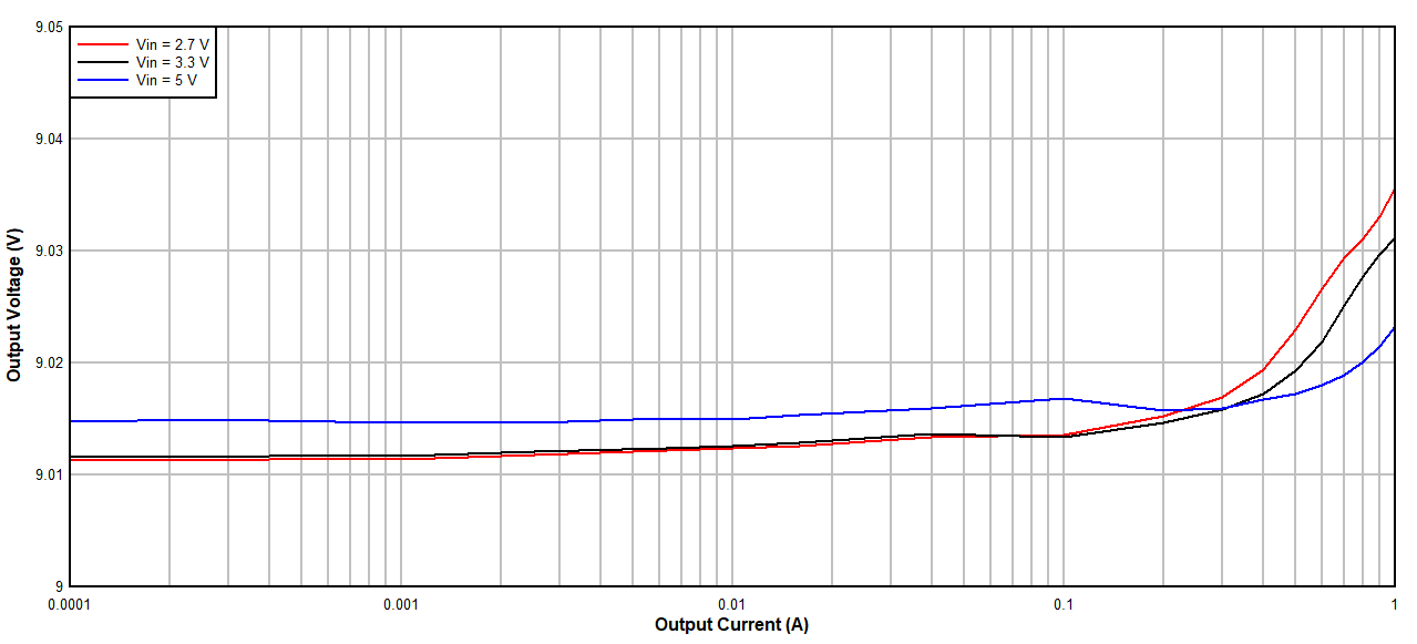
Figure 6-5 9 VOUT
Regulation vs Output Current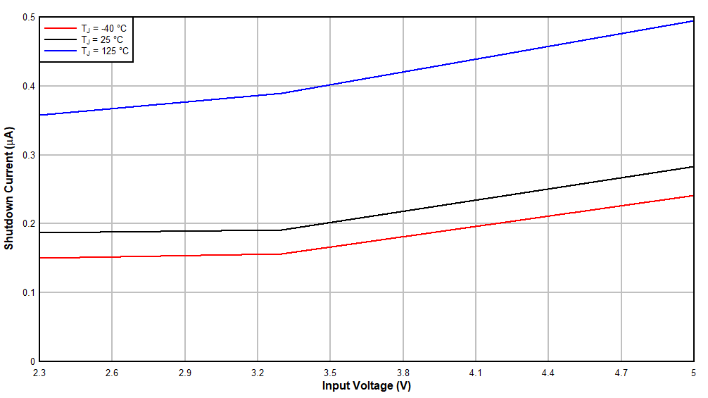 Figure 6-7 Shutdown Current vs Input
Voltage
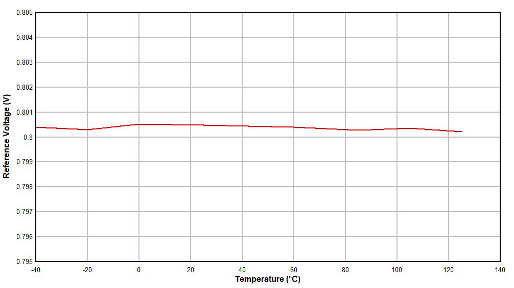 Figure 6-9 Reference Voltage vs
Temperature
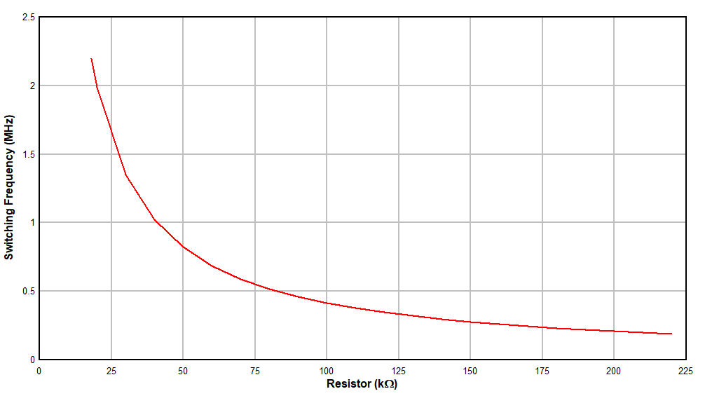 Figure 6-11 Switching Frequency vs
Setting Resistance
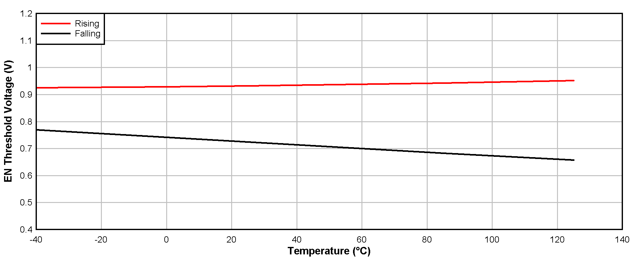 Figure 6-13 EN Threshold Voltage vs
Temperature
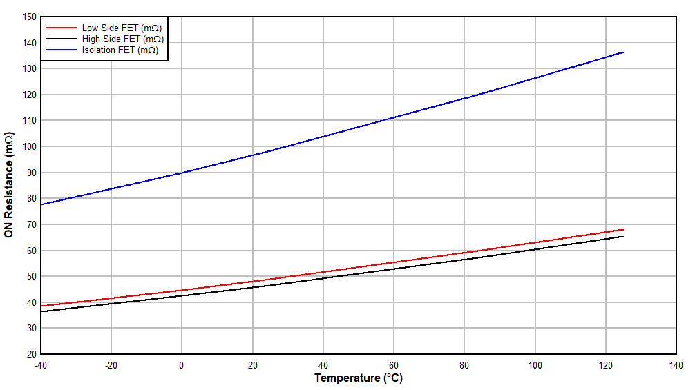 Figure 6-15 RDSON vs
Temperature
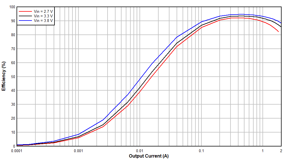
Figure 6-2 5 VOUT
Efficiency vs Output Current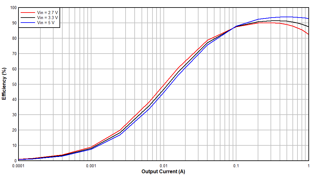
Figure 6-4 9 VOUT
Efficiency vs Output Current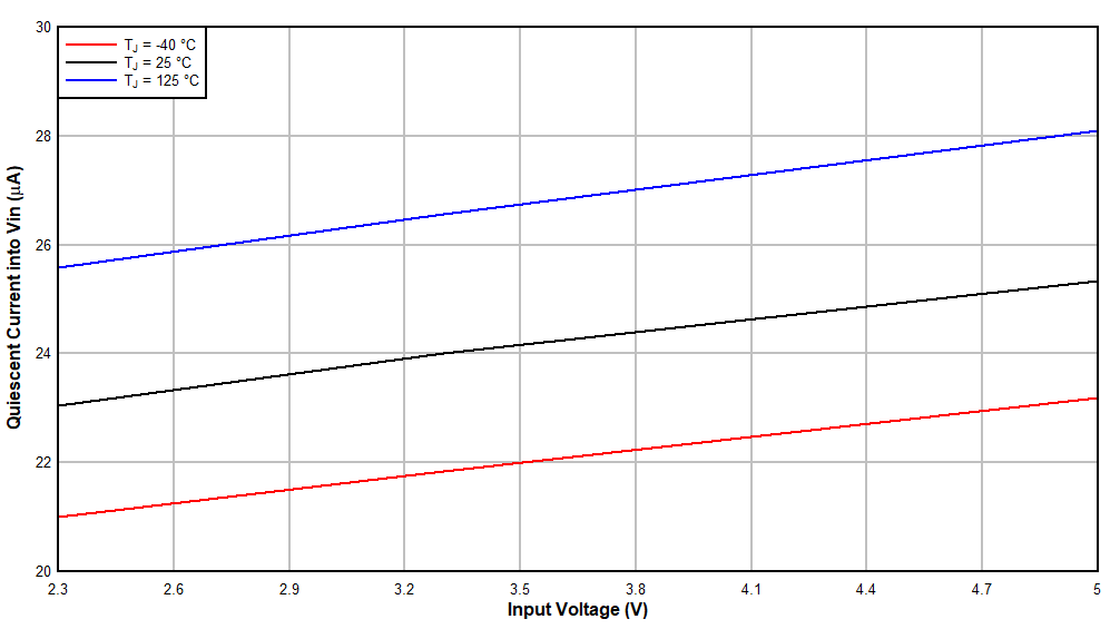 Figure 6-6 Quiescent Current into
VIN vs Input Voltage
 Figure 6-8 Fixed Output Voltage vs
Temperature
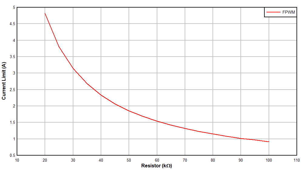 Figure 6-10 Current Limit vs Setting
Resistance
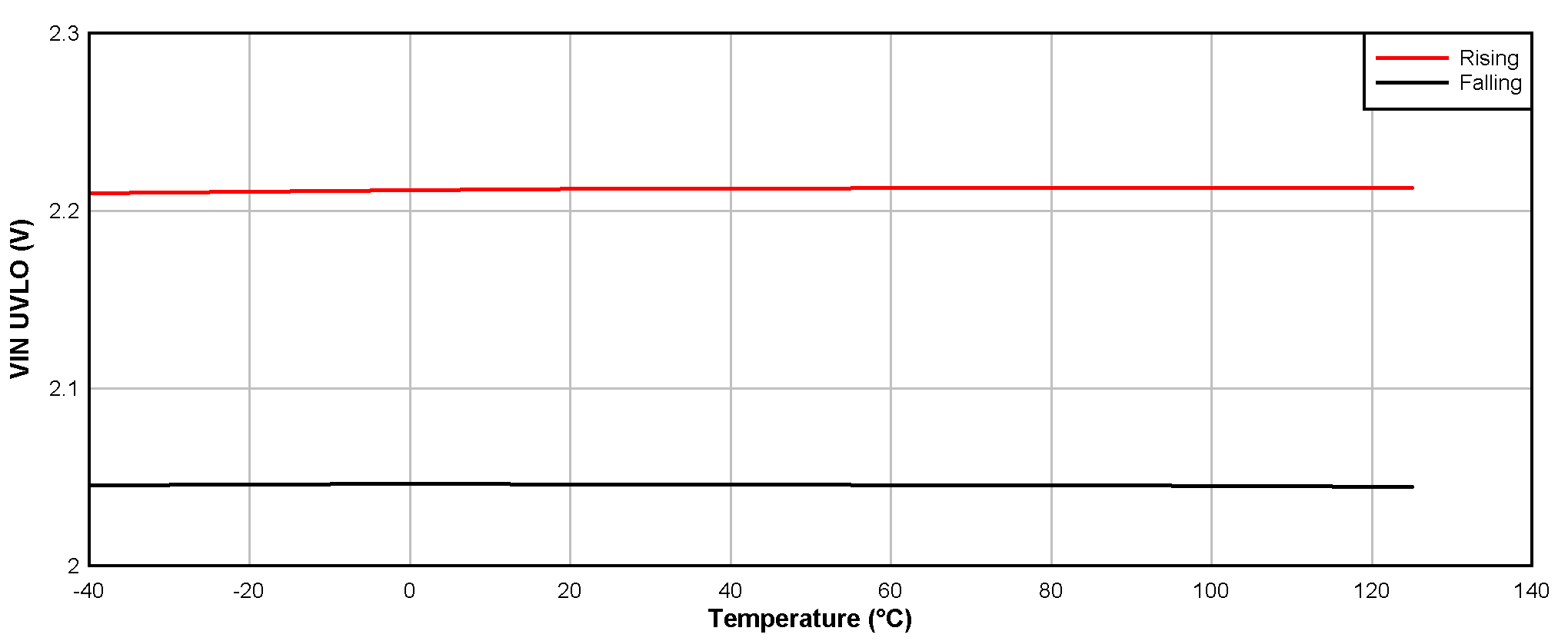 Figure 6-12 VIN UVLO
Threshold Voltage vs Temperature
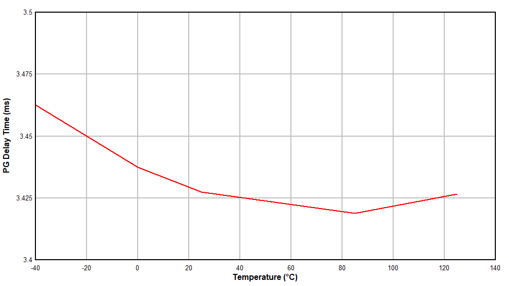 Figure 6-14 PG Delay Time vs
Temperature
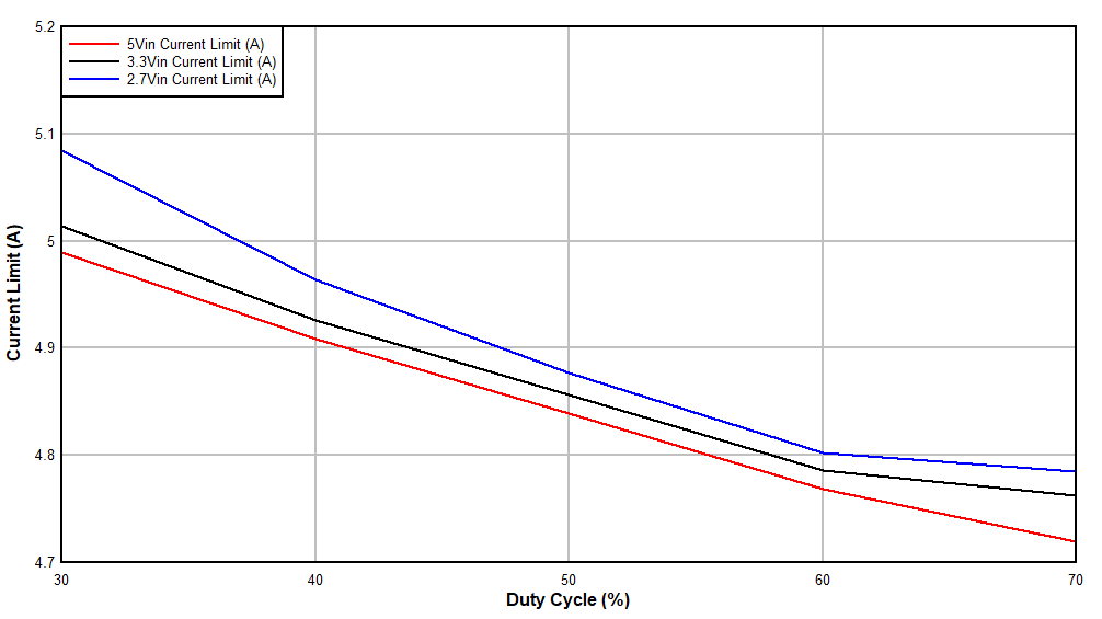 Figure 6-16 Duty Cycle vs Current
Limit

| VOUT = 5 V | Auto PFM | Fsw = 2.2 MHz |

| VOUT = 9 V | Auto PFM | Fsw = 2.2 MHz |

| VOUT = 9 V | PFM | Fsw = 2.2 MHz |
 Figure 6-7 Shutdown Current vs Input
Voltage
 Figure 6-9 Reference Voltage vs
Temperature
 Figure 6-11 Switching Frequency vs
Setting Resistance
 Figure 6-13 EN Threshold Voltage vs
Temperature
 Figure 6-15 RDSON vs
Temperature
| VOUT = 5 V | FPWM | Fsw = 2.2 MHz |

| VOUT = 9 V | FPWM | Fsw = 2.2 MHz |
 Figure 6-6 Quiescent Current into
VIN vs Input Voltage
 Figure 6-8 Fixed Output Voltage vs
Temperature
 Figure 6-10 Current Limit vs Setting
Resistance
 Figure 6-12 VIN UVLO
Threshold Voltage vs Temperature
 Figure 6-14 PG Delay Time vs
Temperature
 Figure 6-16 Duty Cycle vs Current
Limit