SLVSFJ0B March 2021 – October 2021 TPS61379-Q1
PRODUCTION DATA
- 1 Features
- 2 Applications
- 3 Description
- 4 Revision History
- 5 Device Comparison Table
- 6 Pin Configuration and Functions
- 7 Specifications
-
8 Detailed Description
- 8.1 Overview
- 8.2 Functional Block Diagrams
- 8.3
Feature Description
- 8.3.1 VCC Power Supply
- 8.3.2 Input Undervoltage Lockout (UVLO)
- 8.3.3 Enable and Soft Start
- 8.3.4 Shut Down
- 8.3.5 Switching Frequency Setting
- 8.3.6 Spread Spectrum Frequency Modulation
- 8.3.7 Bootstrap
- 8.3.8 Load Disconnect
- 8.3.9 MODE/SYNC Configuration
- 8.3.10 Overvoltage Protection (OVP)
- 8.3.11 Output Short Protection/Hiccup
- 8.3.12 Power-Good Indicator
- 8.3.13 Thermal Shutdown
- 8.4 Device Functional Modes
-
9 Application and Implementation
- 9.1 Application Information
- 9.2
Typical Application
- 9.2.1 Design Requirements
- 9.2.2 Detailed Design Procedure
- 9.2.3 Application Curves
- 10Power Supply Recommendations
- 11Layout
- 12Device and Documentation Support
- 13Mechanical, Packaging, and Orderable Information
Package Options
Mechanical Data (Package|Pins)
- RTE|16
Thermal pad, mechanical data (Package|Pins)
- RTE|16
Orderable Information
8.4.4 Down Mode
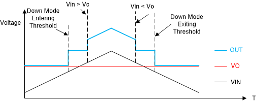
The TPS61379-Q1 features Down mode operation when input voltage is close to or higher than output voltage. In Down mode, output voltage is regulated at target value even when VIN > VO. The high-side and low-side FETs of the TPS61379-Q1 are switching devices that always work in boost operation, where the isolation FET always works as a linear device.
For boost circuits, on time or duty cycle is reduced as input voltage approaches output voltage. The TPS61379-Q1 enters Down mode when VIN reaches 85% (typical) of VO voltage at 2.2 MHz; while exiting Down mode requires VIN to be reduced below 85% (typical) of VO voltage at 2.2 MHz.
In normal operation, isolation FET is fully on.
When Down mode is triggered and VIN is less than VO pin voltage, the OUT pin has a fixed 2 V (typical) above VO pin voltage. Isolation FET works in LDO mode to regulate VO pin voltage with a 2-V constant voltage drop.
When Down mode is triggered and VIN is 100 mV (typical) higher than VO pin voltage, the OUT pin has an approximated 3 V (typical) above VIN pin voltage, as VIN keeps rising, the OUT pin continues to raise with 3 V on top of VIN, isolation FET works in LDO mode to regulate VO pin voltage with a voltage differential of OUT pin and VO pin.
Refer to Figure 8-1.
 Figure 8-1 Down Mode
Care should be taken during short-to-ground condition when operation VIN is above 6 V. During hiccup on, the device operates in Down mode and isolation FET voltage drop is VIN + 3 V (OUT pin to VO pin).