SLVS432F September 2002 – June 2015 TPS62050 , TPS62051 , TPS62052 , TPS62054 , TPS62056
PRODUCTION DATA.
- 1 Features
- 2 Applications
- 3 Description
- 4 Typical Application Schematic
- 5 Revision History
- 6 Device Comparison Table
- 7 Pin Configuration and Functions
- 8 Specifications
- 9 Detailed Description
- 10Application and Implementation
- 11Power Supply Recommendations
- 12Layout
- 13Device and Documentation Support
- 14Mechanical, Packaging, and Orderable Information
Package Options
Refer to the PDF data sheet for device specific package drawings
Mechanical Data (Package|Pins)
- DGS|10
Thermal pad, mechanical data (Package|Pins)
Orderable Information
9 Detailed Description
9.1 Overview
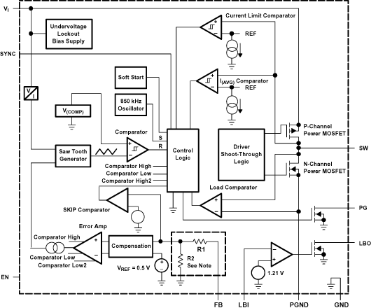
The TPS6205x family of devices are synchronous step-down converters that operate with a 850-kHz fixed-frequency pulse width modulation (PWM) at moderate to heavy load currents and enters the power save mode at light load current.
During PWM operation, the converter uses a unique fast response voltage mode control scheme with input voltage feed forward to achieve good line and load regulation with the use of small ceramic input and output capacitors. At the beginning of each clock cycle initiated by the clock signal (S), the P-channel MOSFET switch is turned on and the inductor current ramps up until the voltage comparator trips and the control logic turns the switch off. Also the switch is turned off by the current limit comparator if the current limit of the P-channel switch is exceeded. After the dead time preventing current shoot through, the N-channel MOSFET rectifier is turned on and the inductor current ramps down. The next cycle is initiated by the clock signal again, turning off the N-channel rectifier and turning on the P-channel switch.
The error amplifier as well as the input voltage determines the rise time of the saw tooth generator; therefore, any change in input voltage or output voltage directly controls the duty cycle of the converter giving a very good line and load transient regulation.
9.2 Functional Block Diagram
9.3 Feature Description
9.3.1 Enable and Overtemperature Protection
A logic low on EN forces the TPS6205x devices into shutdown. In shutdown, the power switch, drivers, voltage reference, oscillator, and all other functions are turned off. The supply current is reduced to less than 2 µA in the shutdown mode. When the device is in thermal shutdown, the bandgap is forced to stay on even if the device is set into shutdown by pulling EN to GND. As soon as the temperature drops below the threshold, the device automatically starts again.
If an output voltage is present when the device is disabled, which could be an external voltage source or super cap, the reverse leakage current is specified under Electrical Characteristics. Pulling the enable pin high starts up the TPS6205x devices with the soft-start as described in Soft-Start. If the EN pin is connected to any voltage other than VI or GND, an increased leakage current of typically 10 µA and up to 20 µA can occur.
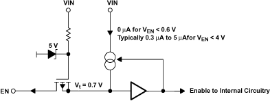 Figure 2. Internal Circuit of the ENABLE Pin
The EN pin can be used in a pushbutton configuration as shown in Figure 3. The external resistor to GND must be capable of sinking 0.3 µA with a minimum voltage drop of 1.3 V to keep the system enabled when both switches are open. When the ON-button is pressed, the device is enabled and the current through the external resistor keeps the voltage level high to ensure that the device stays on when the ON-button is released. When the OFF-button is pressed, the device is switched off and the current through the external resistor is zero. The device therefore stays off even when the OFF-button is released.
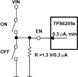 Figure 3. Pushbutton Configuration for the EN-Pin
9.3.2 Low-Battery Detector (Standard Version)
The low-battery output (LBO) is an open-drain type which goes low when the voltage at the low battery input (LBI) falls below the trip point of 1.21 V ±1.5%. The voltage at which the low-battery warning is issued is adjusted with a resistive divider as shown in Figure 5. TI recommends the sum of the resistors R1 and R2 to be in the 100-kΩ to 1-MΩ range for high-efficiency at low output current. An external pullup resistor at LBO can either be connected to OUT, or any other voltage rail in the voltage range of 0 V to 6 V. During start-up, the LBO output signal is invalid for the first 500 µs. LBO is high impedance when the device is disabled. If the low-battery comparator function is not used, connect LBI to ground. The low-battery detector is disabled when the device is disabled. Leave the LBO pin unconnected, or connect to GND when not used.
9.3.3 ENABLE / Low-Battery Detector (Enhanced Version) TPS62051 Only
The TPS62051 device offers an enhanced LBI functionality to provide a precise, user-programmable undervoltage shutdown. No additional supply voltage supervisor (SVS) is needed to provide this function.
When the enable (EN) pin is pulled high, only the internal bandgap voltage reference is switched on to provide a reference source for the LBI comparator. As long as the voltage at LBI is less than the LBI trip point, all other internal circuits are shut down, reducing the supply current to 5 µA. As soon as input voltage at LBI rises above the LBI trip point of 1.21 V, the device is completely enabled and starts switching.
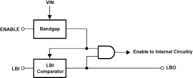 Figure 4. Block Diagram of ENABLE / LBI Functionality for TPS62051
The logic level of the LBO pin is not defined for the first 500 µs after EN is pulled high.
When the enhanced LBI is used to supervise the battery voltage and shut down the TPS62051 at low input voltages, the battery voltage rises again when the current drops to zero. The implemented hysteresis on the LBI pin may not be sufficient for all types of batteries. Figure 5 shows how an additional external hysteresis can be implemented.
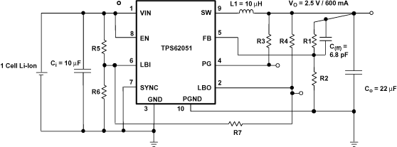 Figure 5. Enhanced LBI With Increased Hysteresis
A MATHCAD® file to calculate R7 can be downloaded from the product folder on the TI web.
9.3.4 Undervoltage Lockout
The undervoltage lockout (UVLO) circuit prevents the device from misoperation at low input voltages. The circuit prevents the converter from turning on the switch or rectifier MOSFET under undefined conditions.
9.3.5 Power Good Comparator
The power good (PG) comparator has an open-drain output capable of sinking typically 1 mA. The PG function is only active when the device is enabled (EN = high). When the device is disabled (EN = low), the PG pin is pulled to GND.
The PG output is only valid after a 250-µs delay after the device is enabled and the supply voltage is greater than 2.7 V. Power good is low during the first 250 µs after shutdown and in shutdown.
The PG pin floats high when the output voltage exceeds typically 98.5% of its nominal value. Leave the PG pin unconnected, or connect it to GND when not used.
9.3.6 Synchronization
If no clock signal is applied, the converter operates with a typical switching frequency of 850 kHz. It is possible to synchronize the converter to an external clock within a frequency range from 600 kHz to 1200 kHz. The device automatically detects the rising edge of the first clock and synchronizes to the external clock. If the clock signal is stopped, the converter automatically switches back to the internal clock and continues operation. The switchover is initiated if no rising edge on the SYNC pin is detected for a duration of four clock cycles. Therefore, the maximum delay time can be 8.3 µs if the internal clock has its minimum frequency of 600 kHz. During this time, there is no clock signal available. The device stops switching until the internal circuitry is switched to the internal clock source.
When the device is switched between internal synchronization and external synchronization during operation, the output voltage may show transient overshoot or undershoot during switchover. The voltage transients are minimized by using 850 kHz as an initial external frequency, and changing the frequency slowly (>1 ms) to the value desired. The voltage drop at the output when the device is switched from external synchronization to internal synchronization can be reduced by increasing the output capacitor value.
If the device is synchronized to an external clock, the power-save mode is disabled and the device stays in forced PWM mode.
Connecting the SYNC pin to the GND pin enables the power-save mode. The converter operates in the PWM mode at moderate to heavy loads and in the PFM mode during light loads maintaining high-efficiency over a wide load current range.
9.4 Device Functional Modes
9.4.1 Soft-Start
The TPS6205x device have an internal soft-start circuit that limits the inrush current during start-up. This prevents possible voltage drops of the input voltage if a battery or a high impedance power source is connected to the input of the TPS6205x devices.
The soft-start is implemented as a digital circuit increasing the switch current in steps of 200 mA, 400 mA, 800 mA and then the typical switch current limit of 1.2 A. Therefore the start-up time mainly depends on the output capacitor and load current. Typical start-up time with a 22-µF output capacitor and a 200-mA load current is 1 ms.
9.4.2 Constant Frequency Mode Operation (SYNC = HIGH)
In the constant frequency mode, the output voltage is regulated by varying the duty cycle of the PWM signal in the range of 100% to 10%. Connecting the SYNC pin to a voltage greater than 1.5 V forces the converter to operate permanently in the PWM mode even at light or no load currents. The advantage is the converter operates with a fixed switching frequency that allows simple filtering of the switching frequency for noise sensitive applications. In this mode, the efficiency is lower compared to the power-save mode during light loads (see Figure 7). The N-MOSFET of the devices stays on even when the current into the output drops to zero. This prevents the device from going into discontinuous mode. The device transfers unused energy back to the input. Therefore, there is no ringing at the output that usually occurs in the discontinuous mode. The duty cycle range in constant frequency mode is 100% to 10%.
It is possible to switch from forced PWM mode to the power-save mode during operation by pulling the SYNC pin low. The flexible configuration of the SYNC pin during operation of the device allows efficient power management by adjusting the operation of the TPS6205x devices to the specific system requirements.
9.4.3 Power-Save Mode Operation (SYNC = LOW)
As the load current decreases, the converter enters the power-save mode operation. During power-save mode the converter operates with reduced switching frequency in PFM and with a minimum quiescent current to maintain high-efficiency. Whenever the average output current goes below the skip threshold, the converter enters the power-save mode. The average current depends on the input voltage. The current is 100 mA at low input voltages and up to 200 mA with maximum input voltage. The average output current must be less than the threshold for at least 32 clock cycles (tcy) to enter the power-save mode. During the power save mode, the output voltage is monitored with a comparator. When the output voltage falls below the comparator low threshold set to 0.8% above VO nominal, the P-channel switch turns on. The P-channel switch turns off as the peak switch current of typically 200 mA is reached. The N-channel rectifier turns on and the inductor current ramps down. As the inductor current approaches zero, the N-channel rectifier is turned off and the switch is turned on starting the next pulse. When the output voltage can not be reached with a single pulse, the device continues to switch with its normal operating frequency, until the comparator detects the output voltage to be 1.6% above the nominal output voltage. The converter wakes up again when the output voltage falls below the comparator low threshold. This control method reduces the quiescent current to typically to 12 µA and the switching frequency to a minimum achieving the highest converter efficiency. Having these skip current thresholds 0.8% and 1.6% above the nominal output voltage gives a lower absolute voltage drop during a load transient as anticipated with a standard converter operating in this mode.
9.4.4 100% Duty Cycle Low Dropout Operation
The TPS6205x devices offer the lowest possible input to output voltage difference while still maintaining operation with the use of the 100% duty cycle mode. In this mode, the P-channel switch is constantly turned on. This is particularly useful in battery-powered applications to achieve longest operation time by taking full advantage of the whole battery voltage range. The minimum input voltage to maintain regulation depends on the load current and output voltage and can be calculated using Equation 1.

9.4.5 No Load Operation
If the converter operates in the forced PWM mode and there is no load connected to the output, the converter regulates the output voltage by allowing the inductor current to reverse for a short period of time.