SLVSD94F November   2017  – November 2024 TPS62088 , TPS62088A , TPS62089A

PRODUCTION DATA  

  1.   1
  2. Features
  3. Applications
  4. Description
  5. Device Options
  6. Pin Configuration and Functions
  7. Specifications
    1. 6.1 Absolute Maximum Ratings 
    2. 6.2 ESD Ratings
    3. 6.3 Recommended Operating Conditions
    4. 6.4 Thermal Information 
    5. 6.5 Electrical Characteristics
    6. 6.6 Typical Characteristics
  8. Detailed Description
    1. 7.1 Overview
    2. 7.2 Functional Block Diagram
    3. 7.3 Feature Description
      1. 7.3.1 Power Save Mode
      2. 7.3.2 Pulse Width Modulation (PWM) Operation
      3. 7.3.3 100% Duty Cycle Low Dropout Operation
      4. 7.3.4 Soft Start
      5. 7.3.5 Switch Current Limit and HICCUP Short-Circuit Protection
      6. 7.3.6 Undervoltage Lockout
      7. 7.3.7 Thermal Shutdown
    4. 7.4 Device Functional Modes
      1. 7.4.1 Enable and Disable
      2. 7.4.2 Power Good
  9. Application and Implementation
    1. 8.1 Application Information
    2. 8.2 Typical Application
      1. 8.2.1 Design Requirements
      2. 8.2.2 Detailed Design Procedure
        1. 8.2.2.1 Custom Design With WEBENCH® Tools
        2. 8.2.2.2 Setting The Output Voltage
        3. 8.2.2.3 Feedforward Capacitor
        4. 8.2.2.4 Output Filter Design
        5. 8.2.2.5 Inductor Selection
        6. 8.2.2.6 Capacitor Selection
      3. 8.2.3 Application Curves
    3. 8.3 Power Supply Recommendations
    4. 8.4 Layout
      1. 8.4.1 Layout Guidelines
      2. 8.4.2 Layout Example
        1. 8.4.2.1 Thermal Considerations
  10. Device and Documentation Support
    1. 9.1 Device Support
      1. 9.1.1 Third-Party Products Disclaimer
      2. 9.1.2 Development Support
        1. 9.1.2.1 Custom Design With WEBENCH® Tools
    2. 9.2 Documentation Support
      1. 9.2.1 Related Documentation
    3. 9.3 Receiving Notification of Documentation Updates
    4. 9.4 Support Resources
    5. 9.5 Trademarks
    6. 9.6 Electrostatic Discharge Caution
    7. 9.7 Glossary
  11. 10Revision History
  12. 11Mechanical, Packaging, and Orderable Information

Package Options

Refer to the PDF data sheet for device specific package drawings

Mechanical Data (Package|Pins)
  • YFP|6
Thermal pad, mechanical data (Package|Pins)
Orderable Information

Description

The TPS6208xx device family is a high-frequency, synchronous step-down converter designed for small design size and high efficiency. With an input voltage range of 2.4V to 5.5V, common battery technologies are supported. At medium to heavy loads, the converter operates in PWM mode and automatically enters power save mode operation at light load to maintain high efficiency over the entire load current range. The forced PWM version of the device maintains a CCM operation across any load. The 4MHz switching frequency allows the device to use small external components. Together with DCS-control architecture, excellent load transient performance, and output voltage regulation accuracy are achieved. Other features like overcurrent protection, thermal shutdown protection, active output discharge, and power good are built in. The device is available in a 6-pin WCSP package.

Device Information
PART NUMBER(2) PACKAGE(1) BODY SIZE (NOM)
TPS62088 YFP (DSBGA, 6) 0.8mm × 1.2mm × 0.5mm
TPS62089A
TPS62088A YWC (DSBGA, 6) 0.8mm × 1.2mm × 0.3mm
For more information, see Section 11.
See the Device Options table.
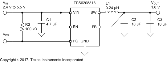
TPS62088 TPS62088A TPS62089A Typical Application SchematicTypical Application Schematic
TPS62088 TPS62088A TPS62089A 3.3V
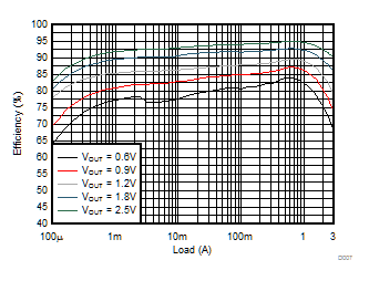
            Input Voltage Efficiency3.3V Input Voltage Efficiency