TPS6240x 2.25-MHz 400-mA and 600-mA Dual Step-Down Converter In Small 3-mm x 3-mm VSON Package
1 Features
- High Efficiency—Up to 95%
- VIN Range From 2.5 V to 6 V
- 2.25-MHz Fixed Frequency Operation
- Output Current of 400 mA and 600 mA
- Adjustable Output Voltage From 0.6V to VIN
- Pin-Selectable Output Voltage Supports Simple Dynamic Voltage Scaling
- EasyScale™ Optional One-Pin Serial Interface
- Power Save Mode at Light Load Currents
- 180° Out-of-Phase Operation
- Output Voltage Accuracy in PWM Mode ±1%
- Typical 32-μA Quiescent Current for Both Converters
- 100% Duty Cycle for Lowest Dropout
- Available in a 10-Pin VSON (3 mm × 3 mm)
2 Applications
- Cell Phones, Smart Phones
- PDAs, Pocket PCs
- OMAP™ and Low-Power DSP Supply
- Portable Media Players
- Digital Radios
- Digital Cameras
3 Description
The TPS6240x family of devices are synchronous dual step-down DC-DC converters optimized for battery-powered portable applications. The devices provide two independent output voltage rails powered by 1-cell Li-Ion or 3-cell NiMH/NiCD batteries. The devices are also suitable to operate from a standard 3.3-V or 5-V voltage rail.
With an input voltage range from 2.5 V to 6 V, the TPS6240x is ideal to power portable applications like smart phones, PDAs, and other portable equipment.
With the EasyScale serial interface the output voltages can be modified during operation. The fixed output voltage versions TPS62401, TPS62402, TPS62403, and TPS62404 support one-pin controlled simple Dynamic Voltage Scaling for low-power processors.
The TPS6240x operates at a 2.25-MHz fixed switching frequency and enters the power save mode operation at light load currents to maintain high efficiency over the entire load current range. For low noise applications the devices can be forced into fixed frequency PWM mode by pulling the MODE/DATA pin high. In the shutdown mode, the current consumption is reduced to 1.2 μA, typical. The devices allow the use of small inductors and capacitors to achieve a small solution size.
The TPS6240x is available in a 10-pin leadless package (3-mm × 3-mm VSON)
Device Information(1)
| PART NUMBER | PACKAGE | BODY SIZE (NOM) |
|---|---|---|
| TPS6240x | VSON (10) | 3.00 mm x 3.00 mm |
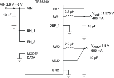
Simplified Schematic
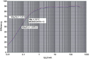
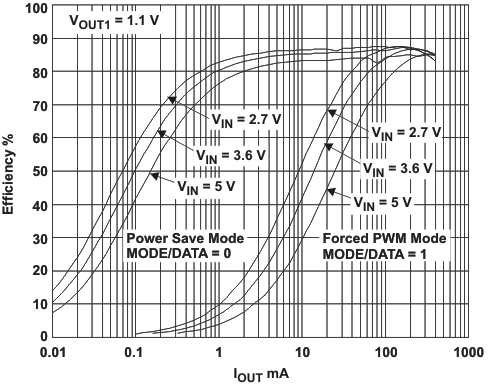
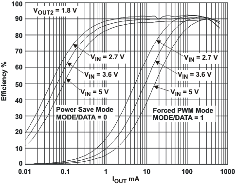
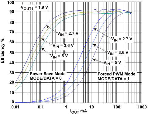
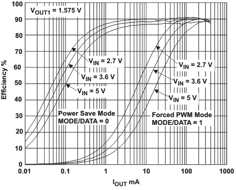
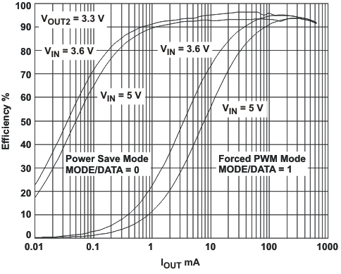
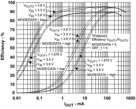
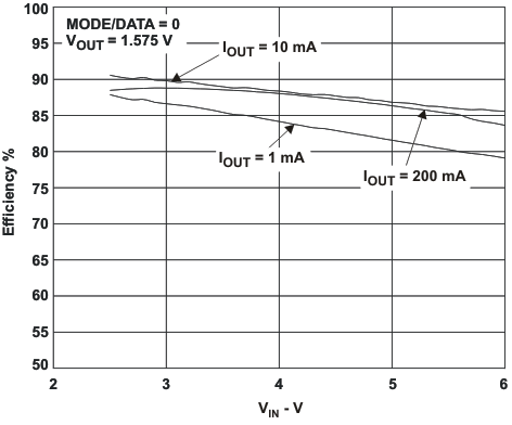
Efficiency vs Output Current
4 Revision History
Changes from E Revision (April 2010) to F Revision
- Added Handling Rating table, Feature Description section, Device Functional Modes, Application and Implementation section, Power Supply Recommendations section, Layout section, Device and Documentation Support section, and Mechanical, Packaging, and Orderable Information sectionGo
Changes from D Revision (February 2006) to E Revision
- Added TPS62404 deviceGo
- Added TPS62404 device to Ordering Information table.Go
- Added TPS62404 device to Addressable Registers table.Go
- Added TPS62404 device to 'Selectable Output Voltages for Converter 1' table.Go
- Added TPS62404 device to 'Selectable Output Voltages for Converter 2' table.Go
- Added TPS62404 device to 'Application Information' section.Go
- Added TPS62404 device efficiency graph (Figure 22).Go
5 Device Options
| TA | PART NUMBER | DEFAULT OUTPUT VOLTAGE(1) | OUTPUT CURRENT | ||
|---|---|---|---|---|---|
| –40 °C to 85 °C | TPS62400 | OUT1 | Adjustable | 400mA | |
| OUT2 | 600mA | ||||
| TPS62401 | OUT1 | Fixed default | DEF_1 = High 1.1V | 400mA | |
| DEF_1 = Low 1.575V | |||||
| OUT2 | Fixed default 1.8V | 600mA | |||
| TPS62402 | OUT1 | Fixed default | DEF_1 = High 1.8V | 400mA | |
| DEF_1 = Low 1.2V | |||||
| OUT2 | Fixed default 3.3V | 600mA | |||
| TPS62403 | OUT1 | Fixed default | DEF_1 = High 1.1V | 400mA | |
| DEF_1 = Low 1.575V | |||||
| OUT2 | Fixed default 2.8V | 600mA | |||
| TPS62404 | OUT1 | Fixed default | DEF_1 = High 1.9V | 400mA | |
| DEF_1 = Low 1.2V | |||||
| OUT2 | Fixed default 3.3V | 600mA | |||
6 Pin Configuration and Functions

Pin Functions
| PIN | I/O | DESCRIPTION | ||
|---|---|---|---|---|
| NAME | NO. | |||
| ADJ2 | 1 | I | Input to adjust output voltage of converter 2. In adjustable version (TPS62400) connect a external resistor divider between VOUT2, this pin and GND to set output voltage between 0.6V and VIN. At fixed output voltage version (TPS62401, TPS62402, TPS62403, TPS62404) this pin MUST be directly connected to the output. If EasyScale Interface is used for converter 2, this pin must be directly connected to the output, too. | |
| DEF_1 | 5 | I | This pin defines the output voltage of converter 1. The pin acts either as analog input for output voltage setting via external resistors (TPS62400), or digital input to select between two fixed default output voltages (TPS62401, TPS62402, TPS62403, TPS62404). | |
| For the TPS62400, an external resistor network needs to be connected to this pin to adjust the default output voltage. | ||||
| Using the fixed output voltage device options this pin selects between two fixed default output voltages, see table ordering information | ||||
| EN1 | 7 | I | Enable Input for Converter1, active high | |
| EN2 | 9 | I | Enable Input for Converter 2, active high | |
| FB1 | 4 | I | Direct feedback voltage sense input of converter 1, connect directly to Vout 1. An internal feed forward capacitor is connected between this pin and the error amplifier. In case of fixed output voltage versions or when the Interface is used, this pin is connected to an internal resistor divider network. | |
| GND | 8 | GND for both converters; connect this pin to the PowerPAD™ | ||
| MODE/DATA | 2 | I/O | This Pin has 2 functions: | |
| 1. | Operation Mode selection: With low level, Power Save Mode is enabled where the device operates in PFM mode at light loads and enters automatically PWM mode at heavy loads. Pulling this PIN to high forces the device to operate in PWM mode over the whole load range. | |||
| 2. | EasyScale™ Interface function: One wire serial interface to change the output voltage of both converters. The pin has an open drain output to provide an acknowledge condition if requested. The current into the open drain output stage may not exceed 500μA. The interface is active if either EN1 or EN2 is high. | |||
| PowerPAD™ | Connect to GND | |||
| SW1 | 6 | I/O | Switch Pin of Converter 1. Connect to Inductor | |
| SW2 | 10 | I/O | Switch Pin of Converter 2. Connect to Inductor. | |
| VIN | 3 | Supply voltage, connect to VBAT, 2.5V to 6V | ||
7 Specifications
7.1 Absolute Maximum Ratings
over operating free-air temperature range (unless otherwise noted)(1)| MIN | MAX | UNIT | |||
|---|---|---|---|---|---|
| Input voltage range on VIN(2) | –0.3 | 7 | V | ||
| Voltage range on EN, MODE/DATA, DEF_1 | –0.3 | VIN +0.3, ≤ 7 | V | ||
| current into MODE/DATA | ≤ 0.5 | mA | |||
| Voltage on SW1, SW2 | –0.3 | 7 | V | ||
| Voltage on ADJ2, FB1 | –0.3 | VIN +0.3, ≤ 7 | V | ||
| TJ(max) | Maximum operating junction temperature | 150 | °C | ||
| TA | Operating ambient temperature range | –40 | 85 | °C | |
7.2 Handling Ratings
| MIN | MAX | UNIT | |||
|---|---|---|---|---|---|
| Tstg | Storage temperature range | –65 | 150 | °C | |
| V(ESD) | Electrostatic discharge(3) | Human body model (HBM), per ANSI/ESDA/JEDEC JS-001, all pins(1) | 1 | kV | |
| Charged device model (CDM), per JEDEC specification JESD22-C101, all pins(2) | 0.5 | ||||
| Machine model | 200 | V | |||
7.3 Recommended Operating Conditions
over operating free-air temperature range (unless otherwise noted)| MIN | NOM | MAX | UNIT | |||
|---|---|---|---|---|---|---|
| VIN | Supply voltage | 2.5 | 6 | V | ||
| VOUT | Output voltage range for adjustable voltage | 0.6 | VIN | V | ||
| TA | Operating ambient temperature | -40 | 85 | °C | ||
| TJ | Operating junction temperature | -40 | 125 | °C | ||
7.4 Thermal Information
| THERMAL METRIC(1) | TPS6240x | UNIT | |
|---|---|---|---|
| VSON | |||
| 10 PINS | |||
| RθJA | Junction-to-ambient thermal resistance | 45.9 | °C/W |
| RθJC(top) | Junction-to-case (top) thermal resistance | 64.3 | |
| RθJB | Junction-to-board thermal resistance | 20.4 | |
| ψJT | Junction-to-top characterization parameter | 1.3 | |
| ψJB | Junction-to-board characterization parameter | 20.6 | |
| RθJC(bot) | Junction-to-case (bottom) thermal resistance | 2.8 | |
7.5 Electrical Characteristics
VIN = 3.6V, VOUT = 1.8V, EN = VIN, MODE = GND, L = 2.2μH, COUT = 20μF, TA = –40°C to 85°C typical values are atTA = 25°C (unless otherwise noted)
| PARAMETER | TEST CONDITIONS | MIN | TYP | MAX | UNIT | ||
|---|---|---|---|---|---|---|---|
| SUPPLY CURRENT | |||||||
| VIN | Input voltage range | 2.5 | 6.0 | V | |||
| IQ | Operating quiescent current | One converter, IOUT = 0mA. PFM mode enabled (Mode = 0) device not switching, EN1 = 1 OR EN2 = 1 |
19 | 29 | μA | ||
| Two converter, IOUT = 0mA. PFM mode enabled (Mode = 0) device not switching, EN1 = 1 AND EN2 = 1 |
32 | 48 | μA | ||||
| IOUT = 0mA, MODE/DATA = GND, for one converter, VOUT 1.575V(1) | 23 | μA | |||||
| IOUT = 0mA, MODE/DATA = VIN, for one converter, VOUT 1.575V (1) | 3.6 | mA | |||||
| ISD | Shutdown current | EN1, EN2 = GND, VIN = 3.6V(2) | 1.2 | 3 | μA | ||
| EN1, EN2 = GND, VIN ramped from 0V to 3.6V(3) | 0.1 | 1 | |||||
| VUVLO | Undervoltage lockout threshold | Falling | 1.5 | 2.35 | V | ||
| Rising | 2.4 | ||||||
| ENABLE EN1, EN2 | |||||||
| VIH | High-level input voltage range, EN1, EN2 | 1.2 | VIN | V | |||
| VIL | Low-level input voltage range, EN1, EN2 | 0 | 0.4 | V | |||
| IIN | Input bias current, EN1, EN2 | EN1, EN2 = GND or VIN | 0.05 | 1.0 | μA | ||
| DEF_1 INPUT | |||||||
| VDEF_1H | DEF_1 high level input voltage range | VOUT1 = fixed output voltage option | 0.9 | VIN | V | ||
| VDEF_1L | DEF_1 low level input voltage range | VOUT1 = fixed output voltage option | 0 | 0.4 | V | ||
| IIN | Input bias current DEF_1 | DEF_1 GND or VIN | 0.01 | 1.0 | μA | ||
| MODE/DATA | |||||||
| VIH | High-level input voltage range, MODE/DATA | 1.2 | VIN | V | |||
| VIL | Low-level input voltage range, MODE/DATA | 0 | 0.4 | V | |||
| IIN | Input bias current, MODE/DATA | MODE/DATA = GND or VIN | 0.01 | 1.0 | μA | ||
| VOH | Acknowledge output voltage high | Open drain, via external pullup resistor | VIN | V | |||
| VOL | Acknowledge output voltage low | Open drain, sink current 500μA | 0 | 0.4 | V | ||
| INTERFACE TIMING | |||||||
| tStart | Start time | 2 | μs | ||||
| tH_LB | High time low bit, logic 0 detection | Signal level on MODE/DATA pin is > 1.2V | 2 | 200 | μs | ||
| tL_LB | Low time low bit, logic 0 detection | Signal level on MODE/DATA pin < 0.4V | 2x tH_LB | 400 | μs | ||
| tL_HB | Low time high bit, logic 1 detection | Signal level on MODE/DATA pin < 0.4V | 2 | 200 | μs | ||
| tH_HB | High time high bit, logic 1 detection | Signal level on MODE/DATA pin is > 1.2V | 2x tL_HB | 400 | μs | ||
| TEOS | End of Stream | TEOS | 2 | μs | |||
| tACKN | Duration of acknowledge condition (MODE/DATE line pulled low by the device) | VIN 2.5V to 6V | 400 | 520 | μs | ||
| tvalACK | Acknowledge valid time | 2 | μs | ||||
| ttimeout | Timeout for entering power save mode | MODE/DATA Pin changes from high to low | 520 | μs | |||
| POWER SWITCH | |||||||
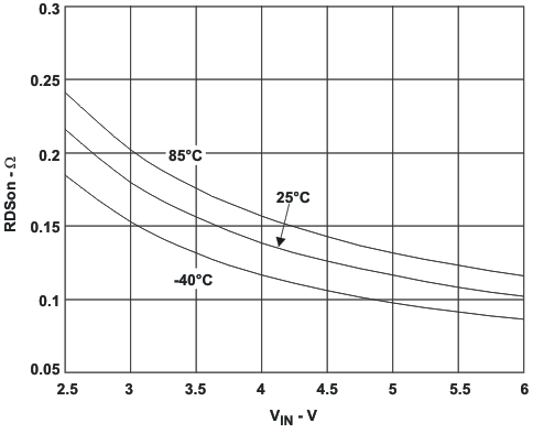
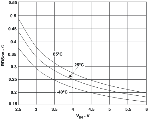
| RDS(ON) | P-Channel MOSFET on-resistance, Converter 1,2 | VIN = VGS = 3.6V | 280 | 620 | mΩ | ||
| ILK_PMOS | P-Channel leakage current | VDS = 6.0V | 1 | μA | |||
| RDS(ON) | N-Channel MOSFET on-resistance Converter 1,2 | VIN = VGS = 3.6V | 200 | 450 | mΩ | ||
| ILK_SW1/SW2 | Leakage current into SW1/SW2 pin | Includes N-Chanel leakage current, VIN = open, VSW = 6.0V, EN = GND(4) |
6 | 7.5 | μA | ||
| ILIMF | Forward Current Limit PMOS and NMOS | OUTPUT 1 | 2.5V ≤ VIN ≤ 6.0V | 0.68 | 0.8 | 0.92 | A |
| OUTPUT 2 | 0.85 | 1.0 | 1.15 | ||||
| TSD | Thermal shutdown | Increasing junction temperature | 150 | °C | |||
| Thermal shutdown hysteresis | Decreasing junction temperature | 20 | °C | ||||
| OSCILLATOR | |||||||
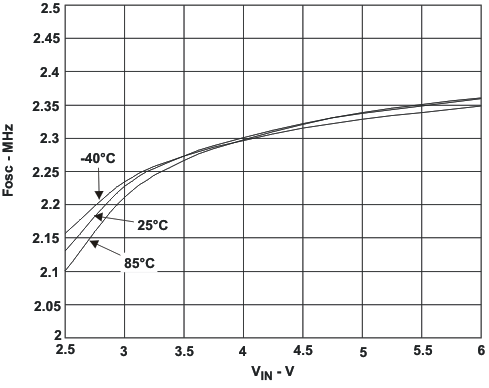
| fSW | Oscillator frequency | 2.5V ≤ VIN ≤ 6V | 2.0 | 2.25 | 2.5 | MHz | |
| OUTPUT | |||||||
| VOUT | Adjustable output voltage range | 0.6 | VIN | V | |||
| Vref | Reference voltage | 600 | mV | ||||
| VOUT (PFM) | DC output voltage accuracy adjustable and fixed output voltage(7) | Voltage positioning active, MODE/DATA = GND, device operating in PFM mode, VIN = 2.5V to 5.0V (5)(8) |
–1.5% | 1.01 VOUT | 2.5% | ||
| VOUT(PWM) | MODE/DATA = GND; device operating in PWM Mode, VIN = 2.5V to 6.0V(8) |
–1% | 0% | 1% | |||
| VIN = 2.5V to 6.0V, Mode/Data = VIN , Fixed PWM operation, 0mA < IOUT1 < 400mA ; 0mA < IOUT2 < 600mA(6) |
–1% | 0% | 1% | ||||
| DC output voltage load regulation | PWM operation mode | 0.5 | %/A | ||||
| tStart up | Start-up time | Activation time to start switching(9) | 170 | μs | |||
| tRamp | VOUT Ramp UP time | Time to ramp from 5% to 95% of VOUT | 750 | μs | |||
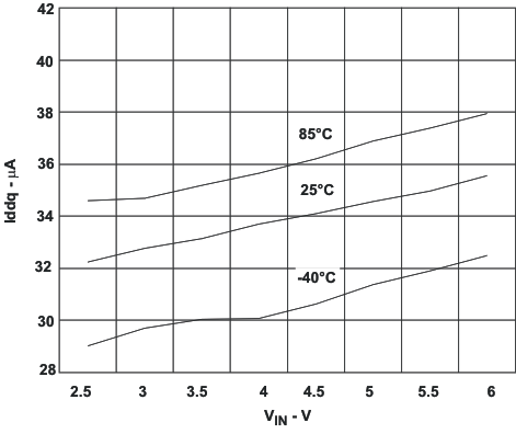
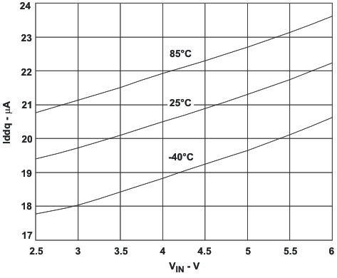
7.6 Typical Characteristics
8 Detailed Description
8.1 Overview
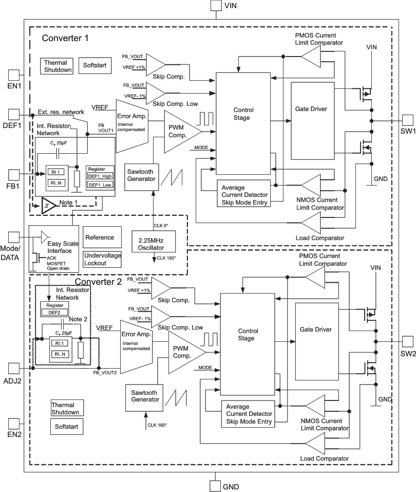
The TPS62400 includes two synchronous step-down converters. The converters operate with typically 2.25MHz fixed frequency pulse width modulation (PWM) at moderate to heavy load currents. If Power Safe Mode is enabled, the converters automatically enter Power Save Mode at light load currents and operate in PFM (Pulse Frequency Modulation).
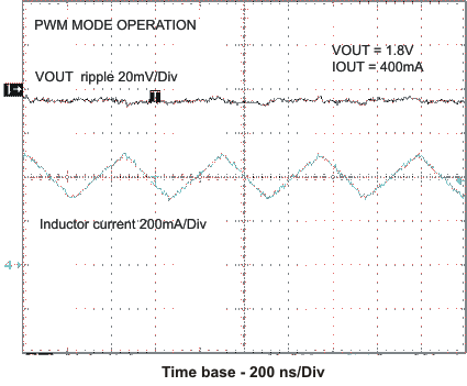
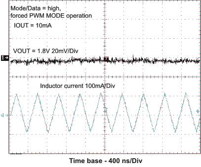
During PWM operation the converters use a unique fast response voltage mode controller scheme with input voltage feed-forward to achieve good line and load regulation allowing the use of small ceramic input and output capacitors. At the beginning of each clock cycle initiated by the clock signal, the P-channel MOSFET switch is turned on and the inductor current ramps up until the comparator trips and the control logic turns off the switch.
Each converter integrates two current limits, one in the P-channel MOSFET and another one in the N-channel MOSFET. When the current in the P-channel MOSFET reaches its current limit, the P-channel MOSFET is turned off and the N-channel MOSFET is turned on. If the current in the N-channel MOSFET is above the N-MOS current limit threshold, the N-channel MOSFET remains on until the current drops below its current limit.
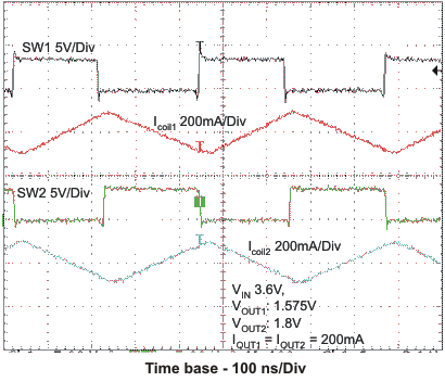
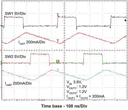
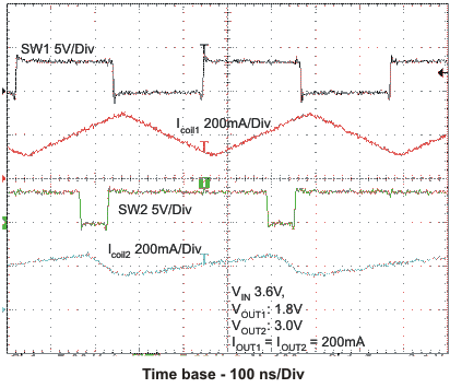
The two DC-DC converters operate synchronized to each other. A 180° phase shift between converter 1 and converter 2 decreases the input RMS current.
8.2 Functional Block Diagram
8.3 Feature Description
8.3.1 Converter 1
In the adjustable output voltage version TPS62400, the converter 1 default output voltage can be set via an external resistor network on PIN DEF_1, which operates as an analog input. In this case, the output voltage can be set in the range of 0.6V to VIN V. The FB1 Pin must be directly connected to the converter 1 output voltage VOUT1. It feeds back the output voltage directly to the regulation loop.
The output voltage of converter 1 can also be changed by the EasyScale™ serial Interface. This makes the device very flexible for output voltage adjustment. In this case, the device uses an internal resistor network.
In the fixed default output voltage version TPS62401, the DEF_1 Pin is configured as a digital input. The converter 1 defaults to 1.1V or 1.575V depending on the level of DEF_1 pin. If DEF_1 is low the default is 1.575V; if high, the default is 1.1V. With the EasyScale™ interface, the output voltage for each DEF_1 Pin condition (high or low) can be changed.
8.3.2 Converter 2
In the adjustable output voltage version TPS62400, the converter 2 output voltage is set by an external resistor divider connected to ADJ2 Pin and uses an external feed forward capacitor of 33pF.
In fixed output voltage version TPS62401, the default output voltage is fixed to 1.8V. In this case, the ADJ2 pin must be connected directly to the converter 2 output voltage VOUT2.
It is also possible to change the output voltage of converter 2 via the EasyScale™ Interface. In this case, the ADJ2 Pin must be directly connected to converter 2 output voltage VOUT2 and no external resistors may be connected.
8.3.3 DEF_1 Pin Function
The DEF_1 pin is dedicated to converter 1 and makes the output voltage selection very flexible to support dynamic voltage management.
Depending on the device version, this pin works either as:
- Analog input for adjustable output voltage setting (TPS62400):
- Connecting an external resistor network to this pin adjusts the default output voltage to any value starting from 0.6V to VIN
- Digital input for fixed default output voltage selection (TPS62401):
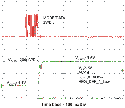
- In case this pin is tied to low level, the output voltage is set according to the value in register REG_DEF_1_Low. The default voltage will be 1.575V. If tied to high level, the output voltage is set according to the value in register REG_DEF_1_High. The default value in this case is 1.1V. Depending on the level of Pin DEF_1, it selects between the two registers REG_DEF_1_Low and REG_DEF_1_High for output voltage setting. Each register content (and therefore output voltage) can be changed individually via the EasyScale™ interface. This makes the device very flexible in terms of output voltage setting; see Table 4.
8.3.4 Mode Selection
The MODE/DATA pin allows mode selection between forced PWM Mode and Power Save Mode for both converters. Furthermore, this pin is a multipurpose pin and provides (besides Mode selection) a one-pin interface to receive serial data from a host to set the output voltage. This is described in the EasyScale™ Interface section.
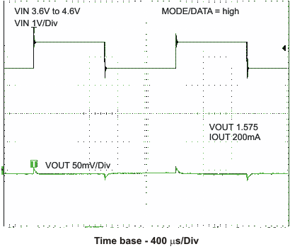
Connecting this pin to GND enables the automatic PWM and power save mode operation. The converters operates in fixed-frequency PWM mode at moderate-to-heavy loads, and in the PFM mode during light loads, maintaining high efficiency over a wide load current range.
Pulling the MODE/DATA pin high forces both converters to operate constantly in the PWM mode, even at light load currents. The advantage is that the converters operate with a fixed frequency, allowing simple filtering of the switching frequency for noise-sensitive applications. In this mode, the efficiency is lower compared to the power save mode during light loads. For additional flexibility, it is possible to switch from power save mode to forced PWM mode during operation. This allows efficient power management by adjusting the operation of the converter to the specific system requirements.
In case the operation mode is changed from forced PWM mode (MODE/DATA = high) to Power Save Mode Enable (MODE/DATA = 0), the Power Save Mode is enabled after a delay time of ttimeout , which is max. 520μs.
The forced PWM Mode operation is enabled immediately with Pin MODE/DATA set to 1.
8.3.5 Enable
The device has a separate EN pin for each converter to start up each converter independently. If EN1 and EN2 are set to high, the corresponding converter starts up with soft start as previously described.
Pulling EN1 and EN2 pin low forces the device into shutdown, with a shutdown quiescent current of typically 1.2μA. In this mode, the P and N-Channel MOSFETs are turned-off and the entire internal control circuitry is switched-off. For proper operation the EN1 and EN2 pins must be terminated and must not be left floating.
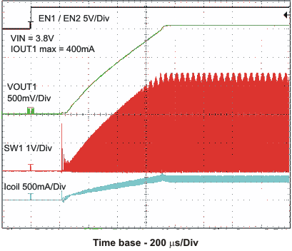
8.3.6 Soft Start
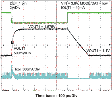
The two converters have an internal soft start circuit that limits the inrush current during start-up. During soft start, the output voltage ramp up is controlled as shown in Figure 6.
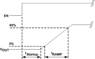 Figure 6. Soft Start
8.3.7 Short-Circuit Protection
Both outputs are short-circuit protected with maximum output current = ILIMF(P-MOS and N-MOS). Once the PMOS switch reaches its current limit, it is turned off and the NMOS switch is turned on. The PMOS only turns on again, once the current in the NMOS decreases below the NMOS current limit.
8.3.8 Under-Voltage Lockout
The under-voltage lockout circuit prevents the device from malfunctioning at low input voltages, and from excessive discharge of the battery, and disables the converters. The under-voltage lockout threshold is typically 1.5V; maximum of 2.35V. In case the default register values are overwritten by the Interface, the new values in the registers REG_DEF_1_High, REG_DEF_1_Low and REG_DEF_2 remain valid as long the supply voltage does not fall below the under-voltage lockout threshold, independent of whether the converters are disabled.
8.3.9 Thermal Shutdown
As soon as the junction temperature, TJ, exceeds 150°C (typical) the device goes into thermal shutdown. In this mode, the P and N-Channel MOSFETs are turned-off. The device continues its operation when the junction temperature falls below the thermal shutdown hysteresis.
8.4 Device Functional Modes
8.4.1 Power Save Mode
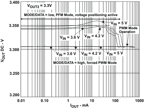
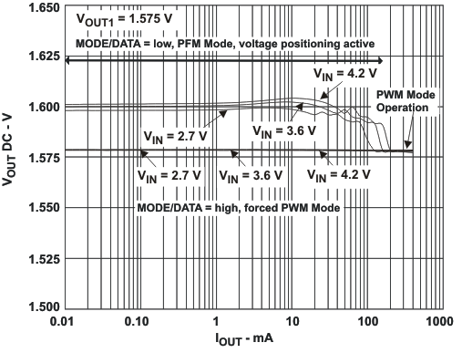
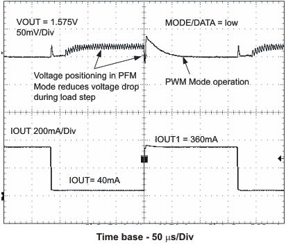
The Power Save Mode is enabled with MODE/DATA Pin set to low for both converters. If the load current of a converter decreases, this converter will enter Power Save Mode operation automatically. The transition to Power Save Mode of a converter is independent from the operating condition of the other converter. During Power Save Mode the converter operates with reduced switching frequency in PFM mode and with a minimum quiescent current to maintain high efficiency. The converter will position the output voltage in PFM mode to typically 1.01×VOUT. This voltage positioning feature minimizes voltage drops caused by a sudden load step.
In order to optimize the converter efficiency at light load the average inductor current is monitored. The device changes from PWM Mode to Power Save Mode, if in PWM mode the inductor current falls below a certain threshold. The typical output current threshold depends on VIN and can be calculated according to Equation 1 for each converter.
Equation 1: Average output current threshold to enter PFM Mode

Equation 2: Average output current threshold to leave PFM Mode

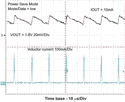
In order to keep the output voltage ripple in Power Save Mode low, the output voltage is monitored with a single threshold comparator (skip comparator). As the output voltage falls below the skip comparator threshold (skip comp) of 1.01 x VOUTnominal, the corresponding converter starts switching for a minimum time period of typ. 1μs and provides current to the load and the output capacitor. Therefore the output voltage will increase and the device maintains switching until the output voltage trips the skip comparator threshold (skip comp) again. At this moment all switching activity is stopped and the quiescent current is reduced to minimum. The load is supplied by the output capacitor until the output voltage has dropped below the threshold again. Hereupon the device starts switching again.
The Power Save Mode is left and PWM Mode entered in case the output current exceeds the current IOUT_PFM_leave or if the output voltage falls below a second comparator threshold, called skip comparator low (Skip Comp Low) threshold. This skip comparator low threshold is set to -2% below nominal Vout, and enables a fast transition from Power Save Mode to PWM Mode during a load step.
In Power Save Mode the quiescent current is reduced typically to 19μA for one converter and 32μA for both converters active. This single skip comparator threshold method in Power Save Mode results in a very low output voltage ripple. The ripple depends on the comparator delay and the size of the output capacitor. Increasing output capacitor values will minimize the output ripple. The Power Save Mode can be disabled through the MODE/DATA pin set to high. Both converters will then operate in fixed PWM mode. Power Save Mode Enable/Disable applies to both converters.
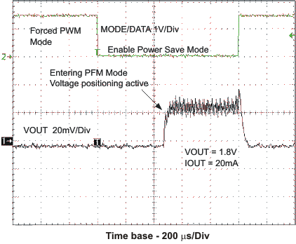
8.4.2 Dynamic Voltage Positioning
This feature reduces the voltage under/overshoots at load steps from light to heavy load and vice versa. It is activated in Power Save Mode operation. It provides more headroom for both the voltage drop at a load step, and the voltage increase at a load throw-off. This improves load transient behavior.
At light loads, in which the converter operates in PFM Mode, the output voltage is regulated typically 1% higher than the nominal value. In case of a load transient from light load to heavy load, the output voltage drops until it reaches the skip comparator low threshold set to –2% below the nominal value and enters PWM mode. During a load throw off from heavy load to light load, the voltage overshoot is also minimized due to active regulation turning on the N-channel switch.
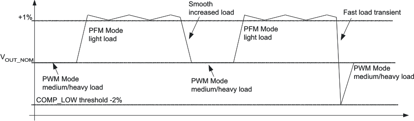 Figure 7. Dynamic Voltage Positioning
8.4.3 100% Duty Cycle Low Dropout Operation
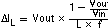
The converters offer a low input-to-output voltage difference while still maintaining operation with the use of the 100% duty cycle mode. In this mode the P-channel switch is constantly turned on. This is particularly useful in battery-powered applications to achieve longest operation time by taking full advantage of the whole battery voltage range. The minimum input voltage to maintain regulation depends on the load current and output voltage, and can be calculated as:

with:
Ioutmax = maximum output current plus inductor ripple current
RDSonmax = maximum P-channel switch RDSon.
RL = DC resistance of the inductor
Voutmax = nominal output voltage plus maximum output voltage tolerance
With decreasing load current, the device automatically switches into pulse skipping operation in which the power stage operates intermittently based on load demand. By running cycles periodically the switching losses are minimized and the device runs with a minimum quiescent current, maintaining high efficiency.
8.4.4 180° Out-Of-Phase Operation
In PWM Mode the converters operate with a 180° turn-on phase shift of the PMOS (high side) transistors. This prevents the high-side switches of both converters from being turned on simultaneously, and therefore smooths the input current. This feature reduces the surge current drawn from the supply.
8.5 Programming
8.5.1 EasyScale™: One-Pin Serial Interface for Dynamic Output Voltage Adjustment
8.5.1.1 General
EasyScale is a simple but very flexible one pin interface to configure the output voltage of both DC-DC converters. The interface is based on a master – slave structure, where the master is typically a microcontroller or application processor. Figure 8 and Table 3. give an overview of the protocol. The protocol consists of a device specific address byte and a data byte. The device specific address byte is fixed to 4E hex. The data byte consists of five bits for information, two address bits, and the RFA bit. RFA bit set to high indicates the Request For Acknowledge condition. The Acknowledge condition is only applied if the protocol was received correctly.
The advantage of EasyScale™ compared to other one pin interfaces is that its bit detection is in a large extent independent from the bit transmission rate. It can automatically detect bit rates between 1.7kBit/sec and up to 160kBit/sec. Furthermore, the interface is shared with the MODE/DATA Pin and requires no additional pin.
8.5.1.2 Protocol
All bits are transmitted MSB first and LSB last. Figure 9 shows the protocol without acknowledge request (bit RFA = 0), Figure 10 with acknowledge (bit RFA = 1) request.
Prior to both bytes, device address byte and data byte, a start condition needs to be applied. For this, the MODE/DATA pin need be pulled high for at least tStart before the bit transmission starts with the falling edge. In case the MODE/DATA line was already at high level (forced PWM Mode selection), no start condition need be applied prior the device address byte.
The transmission of each byte needs to be closed with an End Of Stream condition for at least TEOS.
8.5.1.3 Addressable Registers
Three registers with a data content of 5 bits can be addressed. With 5 bit data content, 32 different values for each register are available. Table 1 shows the addressable registers to set the output voltage when DEF_1 pin works as digital input. In this case, converter 1 has a related register for each DEF_1 Pin condition, and one register for converter 2. With a high/low condition on pin DEF_1 (TPS62401) either the content of register REG_DEF_1_high/REG_DEF1_low is selected. The output voltage of converter 1 is set according to the values in Table 4.
Table 2 shows the addressable registers if DEF_1 pin acts as analog input with external resistors connected. In this case one register is available for each converter. The output voltage of converter 1 is set according to the values in Table 5. For converter 2, the available voltages are shown in Table 6. To generate these output voltages a precise internal resistor divider network is used, making external resistors unnecessary (less board space), and provides higher output voltage accuracy. The Interface is activated if at least one of the converters is enabled (EN1 or EN2 is high). After the startup-time tStart (170μs) the interface is ready for data reception.
Table 1. Addressable Registers for default Fixed Output Voltage Options (PIN DEF_1 = digital input)
| DEVICE | REGISTER | DESCRIPTION | DEF_1 PIN |
A1 | A0 | D4 | D3 | D2 | D1 | D0 |
|---|---|---|---|---|---|---|---|---|---|---|
| TPS62401, TPS62402, TPS62403, TPS62404 | REG_DEF_1_High | Converter 1 output voltage setting for DEF_1 = High condition. The content of the register is active with DEF1_ Pin high. |
High | 0 | 1 | Output voltage setting, see Table 4 | ||||
| REG_DEF_1_Low | Converter 1 output voltage setting for DEF_1 = Low condition. |
Low | 0 | 0 | Output voltage setting, see Table 4 | |||||
| REG_DEF_2 | Converter 2 output voltage | Not applicable | 1 | 0 | Output voltage setting, see Table 6 | |||||
| Don’t use | 1 | 1 | ||||||||
Table 2. Addressable Registers for Adjustable Output Voltage Options (PIN DEF_1 = analog input)
| DEVICE | REGISTER | DESCRIPTION | A1 | A0 | D4 | D3 | D2 | D1 | D0 |
|---|---|---|---|---|---|---|---|---|---|
| TPS62400 | REG_DEF_1_High | not available | |||||||
| REG_DEF_1_Low | Converter 1 output voltage setting | 0 | 0 | see Table 5 | |||||
| REG_DEF_2 | Converter 2 output voltage | 1 | 0 | see Table 6 | |||||
| Don’t’ use | 1 | 1 | |||||||
8.5.1.3.1 Bit Decoding
The bit detection is based on a PWM scheme, where the criterion is the relation between tLOW and tHIGH. It can be simplified to:
High Bit: tHigh > tLow, but with tHigh at least 2x tLow, see Figure 34
Low Bit: tLow> tHigh, but with tLow at least 2x tHigh, see Figure 34
The bit detection starts with a falling edge on the MODE/DATA pin and ends with the next falling edge. Depending on the relation between tLow and tHigh a 0 or 1 is detected.
8.5.1.3.2 Acknowledge
The Acknowledge condition is only applied if:
- Acknowledge is requested by a set RFA bit
- The transmitted device address matches with the device address of the device
- 16 bits were received correctly
In this case, the device turns on the internal ACKN-MOSFET and pulls the MODE/DATA pin low for the time tACKN, which is 520μs maximum . The Acknowledge condition is valid after an internal delay time tvalACK. This means the internal ACKN-MOSFET is turned on after tvalACK, when the last falling edge of the protocol was detected. The master controller keeps the line low during this time.
The master device can detect the acknowledge condition with its input by releasing the MODE/DATA pin after tvalACK and read back a 0.
In case of an invalid device address, or not-correctly-received protocol, no-acknowledge condition is applied; thus, the internal MOSFET is not turned on and the external pullup resistor pulls MODE/DATA pin high after tvalACK. The MODE/DATA pin can be used again after the acknowledge condition ends.
NOTE
The acknowledge condition may only be requested in case the master device has an open drain output.
In case of a push-pull output stage it is recommended to use a series resistor in the MODE/DATA line to limit the current to 500 μA in case of an accidentally requested acknowledge, to protect the internal ACKN-MOSFET.
8.5.1.3.3 MODE Selection
Because the MODE/DATA pin is used for two functions, interface and a MODE selection, the device needs to determine when it has to decode the bit stream or to change the operation mode.
The device enters forced PWM mode operation immediately whenever the MODE/DATA pin turns to high level. The device also stays in forced PWM mode during the entire protocol reception time.
With a falling edge on the MODE/DATA pin the device starts bit decoding. If the MODE/DATA pin stays low for at least ttimeout, the device gets an internal timeout and Power Save Mode operation is enabled.
A protocol sent within this time is ignored because the falling edge for the Mode change is first interpreted as start of the first bit. In this case it is recommended to send the protocol first, and then change at the end of the protocol to Power Save Mode.
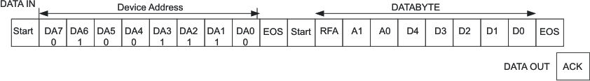 Figure 8. EasyScale™ Protocol Overview
Table 3. EasyScale™ Bit Description
| BYTE | BIT NUMBER | NAME | TRANSMISSION DIRECTION | DESCRIPTION |
|---|---|---|---|---|
| Device Address Byte | 7 | DA7 | IN | 0 MSB device address |
| 6 | DA6 | IN | 1 | |
| 5 | DA5 | IN | 0 | |
| 4 | DA4 | IN | 0 | |
| 4Ehex | 3 | DA3 | IN | 1 |
| 2 | DA2 | IN | 1 | |
| 1 | DA1 | IN | 1 | |
| 0 | DA0 | IN | 0 LSB device address | |
| Databyte | 7(MSB) | RFA | IN | Request For Acknowledge, if high, Acknowledge condition will applied by the device |
| 6 | A1 | Address Bit 1 | ||
| 5 | A0 | Address Bit 0 | ||
| 4 | D4 | Data Bit 4 | ||
| 3 | D3 | Data Bit 3 | ||
| 2 | D2 | Data Bit 2 | ||
| 1 | D1 | Data Bit 1 | ||
| 0(LSB) | D0 | Data Bit 0 | ||
| ACK | OUT | Acknowledge condition active 0, this condition will only be applied in case RFA bit is set. Open drain output, Line needs to be pulled high by the host with a pullup resistor. | ||
| This feature can only be used if the master has an open drain output stage. In case of a push pull output stage Acknowledge condition may not be requested! |
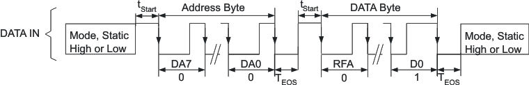 Figure 9. EasyScale™ Protocol Without Acknowledge
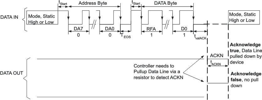 Figure 10. EasyScale™ Protocol Including Acknowledge
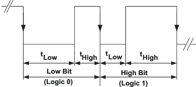 Figure 11. EasyScale™ – Bit Coding
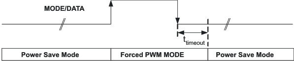 Figure 12. MODE/DATA PIN: Mode Selection
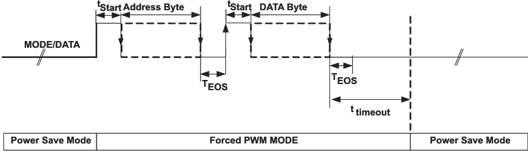 Figure 13. MODE/DATA Pin: Power Save Mode/Interface Communication
Table 4. Selectable Output Voltages for Converter 1,
With Pin DEF_1 as Digital Input (TPS62401)
Table 5. Selectable Output Voltages for Converter 1,
With DEF1 Pin as Analog Input (Adjustable, TPS62400)
| TPS62400 OUTPUT VOLTAGE [V] REGISTER REG_DEF_1_LOW |
D4 | D3 | D2 | D1 | D0 | |
|---|---|---|---|---|---|---|
| 0 | VOUT1 Adjustable with Resistor Network on DEF_1 Pin (default TPS62400) | 0 | 0 | 0 | 0 | 0 |
| 0.6V with DEF_1 connected to VOUT1 (default TPS62400) | ||||||
| 1 | 0.825 | 0 | 0 | 0 | 0 | 1 |
| 2 | 0.85 | 0 | 0 | 0 | 1 | 0 |
| 3 | 0.875 | 0 | 0 | 0 | 1 | 1 |
| 4 | 0.9 | 0 | 0 | 1 | 0 | 0 |
| 5 | 0.925 | 0 | 0 | 1 | 0 | 1 |
| 6 | 0.95 | 0 | 0 | 1 | 1 | 0 |
| 7 | 0.975 | 0 | 0 | 1 | 1 | 1 |
| 8 | 1.0 | 0 | 1 | 0 | 0 | 0 |
| 9 | 1.025 | 0 | 1 | 0 | 0 | 1 |
| 10 | 1.050 | 0 | 1 | 0 | 1 | 0 |
| 11 | 1.075 | 0 | 1 | 0 | 1 | 1 |
| 12 | 1.1 | 0 | 1 | 1 | 0 | 0 |
| 13 | 1.125 | 0 | 1 | 1 | 0 | 1 |
| 14 | 1.150 | 0 | 1 | 1 | 1 | 0 |
| 15 | 1.175 | 0 | 1 | 1 | 1 | 1 |
| 16 | 1.2 | 1 | 0 | 0 | 0 | 0 |
| 17 | 1.225 | 1 | 0 | 0 | 0 | 1 |
| 18 | 1.25 | 1 | 0 | 0 | 1 | 0 |
| 19 | 1.275 | 1 | 0 | 0 | 1 | 1 |
| 20 | 1.3 | 1 | 0 | 1 | 0 | 0 |
| 21 | 1.325 | 1 | 0 | 1 | 0 | 1 |
| 22 | 1.350 | 1 | 0 | 1 | 1 | 0 |
| 23 | 1.375 | 1 | 0 | 1 | 1 | 1 |
| 24 | 1.4 | 1 | 1 | 0 | 0 | 0 |
| 25 | 1.425 | 1 | 1 | 0 | 0 | 1 |
| 26 | 1.450 | 1 | 1 | 0 | 1 | 0 |
| 27 | 1.475 | 1 | 1 | 0 | 1 | 1 |
| 28 | 1.5 | 1 | 1 | 1 | 0 | 0 |
| 29 | 1.525 | 1 | 1 | 1 | 0 | 1 |
| 30 | 1.55 | 1 | 1 | 1 | 1 | 0 |
| 31 | 1.575 | 1 | 1 | 1 | 1 | 1 |
Table 6. Selectable Output Voltages for Converter 2,
(ADJ2 Connected to VOUT)
9 Application and Implementation
9.1 Application Information
The TPS6240x family of devices are synchronous dual step-down DC-DC converters. The devices provide two independent output voltage rails. The following information gives guidance on choosing external components to complete the application design.
9.2 Typical Applications
9.2.1 TPS6240x, Dual Outputs Step Down Converter
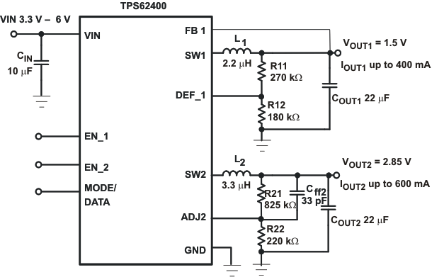 Figure 14. Typical Application Circuit 1.5V/2.85V Adjustable Outputs, Low PFM Voltage Ripple Optimized
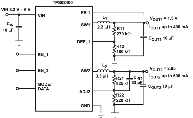 Figure 15. Typical Application Circuit 1.5V/2.85V Adjustable Outputs
9.2.1.1 Design Requirements
The step-down converter design can be adapted to different output voltage and load current needs by choosing external components appropriate. The following design procedure is adequate for whole VIN, VOUT and load current range of TPS6240x.
9.2.1.2 Detailed Design Procedure
9.2.1.2.1 Converter1 Adjustable Default Output Voltage Setting: TPS62400
The output voltage can be calculated to:

To keep the operating current to a minimum, it is recommended to select R12 within a range of 180kΩ to 360kΩ. The sum of R12 and R11 should not exceed ~1MΩ. For higher output voltages than 3.3V, it is recommended to choose lower values than 180kΩ for R12. Route the DEF_1 line away from noise sources, such as the inductor or the SW1 line. The FB1 line needs to be directly connected to the output capacitor. A feed-forward capacitor is not necessary.
9.2.1.2.2 Converter1 Fixed Default Output Voltage Setting (TPS62401, TPS62402, TPS62403, TPS62404).
The output voltage VOUT1 is selected with DEF_1 pin.
Pin DEF_1 = low:
TPS62401, TPS62403 = 1.575V
Pin DEF_1 = high:
TS62401, TPS62403 = 1.1V
T62402: = 1.8V
T62404: = 1.9V
9.2.1.2.3 Converter 2 Adjustable Default Output Voltage Setting TPS62400:
The output voltage of converter 2 can be set by an external resistor network. For converter 2 the same recommendations apply as for converter1. In addition to that, a 33pF feed-forward Capacitor Cff2 for good load transient response should be used. The output voltage can be calculated to:

9.2.1.2.4 Converter 2 Fixed Default Output Voltage Setting
ADJ2 pin must be directly connected with VOUT2
TPS62401, VOUT2 default = 1.8V
TPS62403, VOUT2 default = 2.8V
TPS62402, TPS62404, VOUT2 default = 3.3V
9.2.1.2.5 Output Filter Design (Inductor and Output Capacitor)
The converters are designed to operate with a minimum inductance of 1.75μH and minimum capacitance of 6μF. The device is optimized to operate with inductors of 2.2μH to 4.7μH and output capacitors of 10μF to 22μF.
9.2.1.2.5.1 Inductor Selection
The selected inductor has to be rated for its DC resistance and saturation current. The DC resistance of the inductor will influence directly the efficiency of the converter. Therefore an inductor with lowest DC resistance should be selected for highest efficiency.
Equation 6 calculates the maximum inductor current under static load conditions. The saturation current of the inductor should be rated higher than the maximum inductor current as calculated with Equation 7. This is recommended because during heavy load transient the inductor current rises above the calculated value.
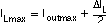
with:
f = Switching Frequency (2.25MHz typical)
L = Inductor Value
ΔIL = Peak-to-Peak inductor ripple current
ILmax = Maximum Inductor current
The highest inductor current occurs at maximum Vin.
Open core inductors have a soft saturation characteristic and they can usually handle higher inductor currents versus a comparable shielded inductor.
A more conservative approach is to select the inductor current rating just for the maximum switch current of the corresponding converter. Take into consideration that the core material from inductor to inductor differs and this difference has an impact on the efficiency.
Refer to Table 7 and the typical application circuit examples for possible inductors.
Table 7. List of Inductors
| DIMENSIONS [mm3] | INDUCTOR TYPE | SUPPLIER |
|---|---|---|
| 3.2×2.6×1.0 | MIPW3226 | FDK |
| 3×3×0.9 | LPS3010 | Coilcraft |
| 2.8×2.6×1.0 | VLF3010 | TDK |
| 2.8x2.6×1.4 | VLF3014 | TDK |
| 3×3×1.4 | LPS3015 | Coilcraft |
| 3.9×3.9×1.7 | LPS4018 | Coilcraft |
9.2.1.2.5.2 Output Capacitor Selection
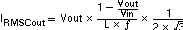
The advanced fast response voltage mode control scheme of the converters allows the use of tiny ceramic capacitors with a typical value of 10μF to 22μF, without having large output voltage under and overshoots during heavy load transients. Ceramic capacitors with low ESR values results in lowest output voltage ripple, and are therefore recommended. The output capacitor requires either X7R or X5R dielectric. Y5V and Z5U dielectric capacitors are not recommended due to their wide variation in capacitance.
If ceramic output capacitors are used, the capacitor RMS ripple current rating always meets the application requirements. The RMS ripple current is calculated as:
At nominal load current the inductive converters operate in PWM mode and the overall output voltage ripple is the sum of the voltage spike caused by the output capacitor ESR, plus the voltage ripple caused by charging and discharging the output capacitor:
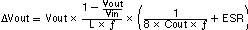
Where the highest output voltage ripple occurs at the highest input voltage Vin.
At light load currents the converters operate in Power Save Mode and the output voltage ripple is dependent on the output capacitor value. The output voltage ripple is set by the internal comparator delay and the external capacitor. Higher output capacitors like 22μF values minimize the voltage ripple in PFM Mode and tighten DC output accuracy in PFM Mode.
9.2.1.2.5.3 Input Capacitor Selection
Because of the nature of the buck converter having a pulsating input current, a low ESR input capacitor is required to prevent large voltage transients that can cause misbehavior of the device or interference with other circuits in the system. An input capacitor of 10μF is sufficient.
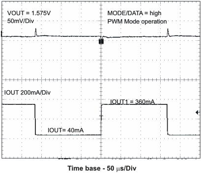
9.2.1.3 Application Curves
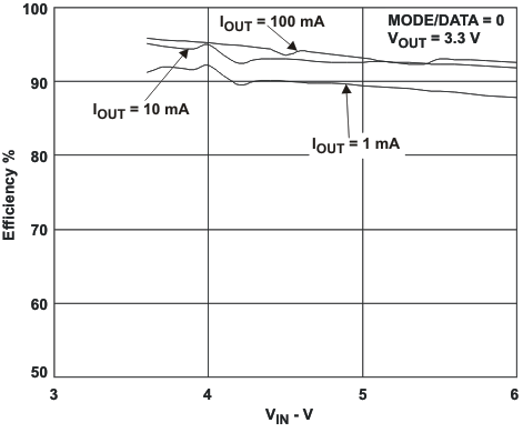
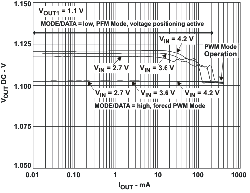
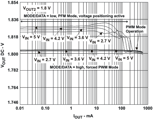
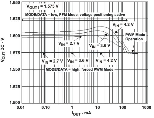
VIN = 3.6 V, and TA = 25 °C, unless otherwise noted.
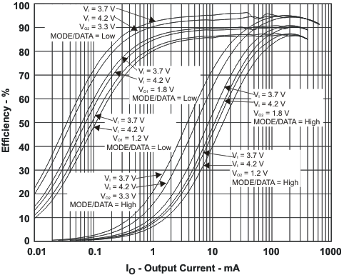
L = 2.2μH, COUT = 22μF
VOUT1 = 1.575V, VOUT2 = 1.8V
VOUT1 = 1.2V, VOUT2 = 1.2V
L = 3.3μH, COUT = 10μF
VOUT1 = 1.8V, VOUT2 = 3.0V
9.2.2 Various Output Voltages
The TPS6240x is able to be set for different output voltages. Some examples are shown below.
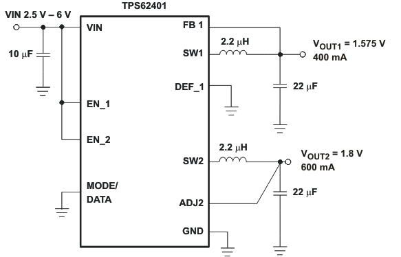 Figure 42. TPS62401 Fixed 1.575V/1.8V Outputs, Low PFM Voltage Ripple Optimized
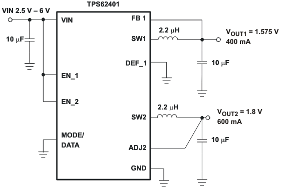 Figure 43. TPS62401 Fixed 1.575V/1.8V Outputs
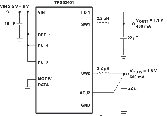 Figure 44. TPS62401 Fixed 1.1V/1.8V Outputs, Low PFM Ripple Voltage Optimized
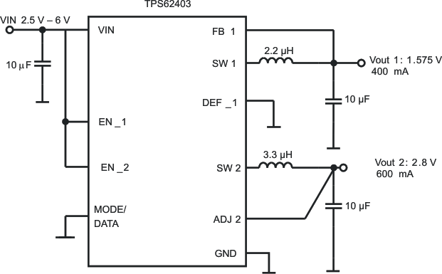 Figure 45. TPS62403 1.575V/2.8V Outputs
9.2.2.1 Design Requirements
The TPS6240x step-down converter is set to different output voltages.
9.2.2.2 Detailed Design Procedure
9.2.3 Dynamic Voltage Scaling on Converter 1 by DEF_1 Pin
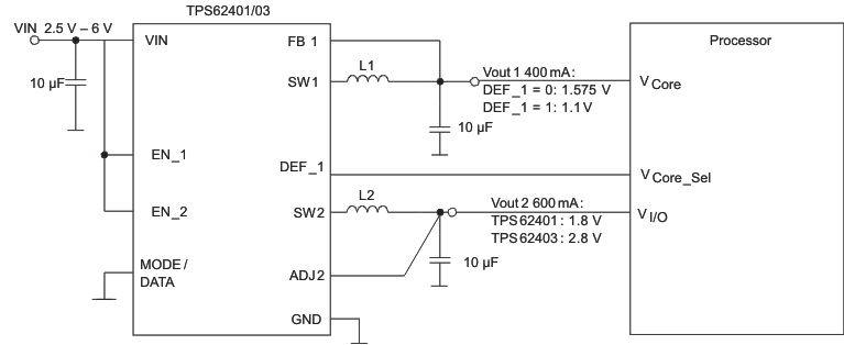 Figure 46. Dynamic Voltage Scaling on Converter 1 by DEF_1 Pin
9.2.3.1 Design Requirements
Control the output voltage of the converter 1 through DEF_1 pin by an external processor.
9.2.3.2 Detailed Design Procedure
Connect the DEF_1 pin to the VCore_Sel pin of an external processor, as shown in Figure 46. The processor determines the logic status of the DEF_1 pin which sets the output voltage of the converter 1.
Application Curves