SLVSFM8 March 2021 TPS62810M , TPS62811M , TPS62812M , TPS62813M
PRODUCTION DATA
- 1 Features
- 2 Applications
- 3 Description
- 4 Revision History
- 5 Device Comparison Table
- 6 Pin Configuration and Functions
- 7 Specifications
- 8 Parameter Measurement Information
- 9 Detailed Description
- 10Application and Implementation
- 11Power Supply Recommendations
- 12Layout
- 13Device and Documentation Support
- 14Mechanical, Packaging, and Orderable Information
Package Options
Mechanical Data (Package|Pins)
- RWY|9
Thermal pad, mechanical data (Package|Pins)
- RWY|9
Orderable Information
3 Description
The TPS6281xM is family of pin-to-pin 1-A, 2-A, 3-A, and 4-A synchronous step-down DC/DC converters. All devices offer high efficiency and ease of use. The family of devices is based on a peak current mode control topology. Low-resistive switches allow up to 4-A continuous output current at high ambient temperature. The switching frequency is externally adjustable from 1.8 MHz to 4 MHz and can also be synchronized to an external clock in the same frequency range. The device can automatically enter power save mode (PSM) at light loads to maintain high efficiency across the whole load range. The device provides 1% output voltage accuracy in PWM mode which helps design a power supply with high output voltage accuracy. The SS/TR pin allows the user to set the start-up time or form tracking of the output voltage to an external source, allowing external sequencing of different supply rails and limiting the inrush current during start-up.
The TPS6281xM device is available in a 2-mm × 3-mm VQFN package with wettable flanks.
| PART NUMBER | PACKAGE(1) | BODY SIZE (NOM) |
|---|---|---|
| TPS62810M | VQFN | 2 mm × 3 mm |
| TPS62811M | ||
| TPS62812M | ||
| TPS62813M |
 Simplified Schematic
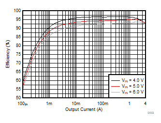
 Efficiency Versus Output Current;
 VOUT = 3.3 V; PWM and PFM; fS = 2.25 MHz