SLUSEC8B March 2021 – April 2024 TPS628501 , TPS628502 , TPS628503
PRODUCTION DATA
- 1
- 1 Features
- 2 Applications
- 3 Description
- 4 Device Comparison Table
- 5 Pin Configuration and Functions
- 6 Specifications
- 7 Parameter Measurement Information
-
8 Detailed Description
- 8.1 Overview
- 8.2 Functional Block Diagram
- 8.3 Feature Description
- 8.4
Device Functional Modes
- 8.4.1 Pulse Width Modulation (PWM) Operation
- 8.4.2 Power Save Mode Operation (PWM/PFM)
- 8.4.3 100% Duty-Cycle Operation
- 8.4.4 Current Limit and Short Circuit Protection
- 8.4.5 Foldback Current Limit and Short Circuit Protection
- 8.4.6 Output Discharge
- 8.4.7 Soft Start
- 8.4.8 Input Overvoltage Protection
- 9 Application and Implementation
- 10Device and Documentation Support
- 11Revision History
- 12Mechanical, Packaging, and Orderable Information
Package Options
Mechanical Data (Package|Pins)
- DRL|8
Thermal pad, mechanical data (Package|Pins)
Orderable Information
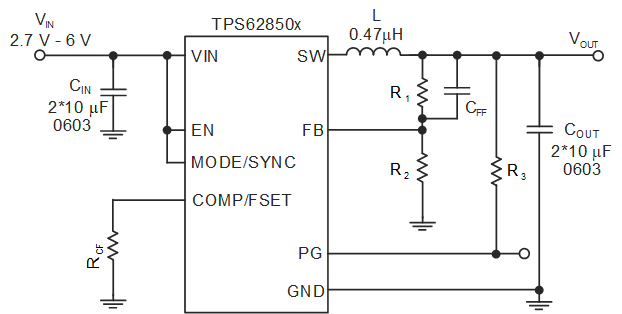
9.2 Typical Application
 Figure 9-1 Typical
Application