SLUSEC8B March 2021 – April 2024 TPS628501 , TPS628502 , TPS628503
PRODUCTION DATA
- 1
- 1 Features
- 2 Applications
- 3 Description
- 4 Device Comparison Table
- 5 Pin Configuration and Functions
- 6 Specifications
- 7 Parameter Measurement Information
-
8 Detailed Description
- 8.1 Overview
- 8.2 Functional Block Diagram
- 8.3 Feature Description
- 8.4
Device Functional Modes
- 8.4.1 Pulse Width Modulation (PWM) Operation
- 8.4.2 Power Save Mode Operation (PWM/PFM)
- 8.4.3 100% Duty-Cycle Operation
- 8.4.4 Current Limit and Short Circuit Protection
- 8.4.5 Foldback Current Limit and Short Circuit Protection
- 8.4.6 Output Discharge
- 8.4.7 Soft Start
- 8.4.8 Input Overvoltage Protection
- 9 Application and Implementation
- 10Device and Documentation Support
- 11Revision History
- 12Mechanical, Packaging, and Orderable Information
Package Options
Mechanical Data (Package|Pins)
- DRL|8
Thermal pad, mechanical data (Package|Pins)
Orderable Information
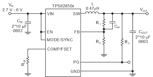
7.1 Schematic
 Figure 7-1 Measurement Setup
Table 7-1 List of Components
| REFERENCE | DESCRIPTION | MANUFACTURER (1) |
|---|---|---|
| IC | TPS628502 | Texas Instruments |
| L | 0.47-µH inductor DFE252012PD | Murata |
| CIN | 2 × 10 µF / 6.3 V GRM188D70J106MA73 | Murata |
| COUT | 2 × 10 µF / 6.3 V GRM188D70J106MA73 for VOUT ≥ 1 V | Murata |
| COUT | 3 × 10 µF / 6.3 V GRM188D70J106MA73 for VOUT < 1 V | Murata |
| RCF | 8.06 kΩ | Any |
| CFF | 10 pF | Any |
| R1 | Depending on VOUT | Any |
| R2 | Depending on VOUT | Any |
| R3 | 100 kΩ | Any |
(1) See the Third-party Products Disclaimer.