SLUSDM0K May   2020  – June 2024 TPS628501-Q1 , TPS628502-Q1 , TPS628503-Q1

PRODMIX  

  1.   1
  2. Features
  3. Applications
  4. Description
  5. Device Comparison Table
  6. Pin Configuration and Functions
  7. Specifications
    1. 6.1 Absolute Maximum Ratings
    2. 6.2 ESD Ratings
    3. 6.3 Recommended Operating Conditions
    4. 6.4 Thermal Information
    5. 6.5 Electrical Characteristics
    6. 6.6 Typical Characteristics
  8. Parameter Measurement Information
    1. 7.1 Schematic
  9. Detailed Description
    1. 8.1 Overview
    2. 8.2 Functional Block Diagram
    3. 8.3 Feature Description
      1. 8.3.1 Precise Enable (EN)
      2. 8.3.2 COMP/FSET
      3. 8.3.3 MODE / SYNC
      4. 8.3.4 Spread Spectrum Clocking (SSC)
      5. 8.3.5 Undervoltage Lockout (UVLO)
      6. 8.3.6 Power-Good Output (PG)
      7. 8.3.7 Thermal Shutdown
    4. 8.4 Device Functional Modes
      1. 8.4.1 Pulse Width Modulation (PWM) Operation
      2. 8.4.2 Power Save Mode Operation (PWM/PFM)
      3. 8.4.3 100% Duty-Cycle Operation
      4. 8.4.4 Current Limit and Short Circuit Protection
      5. 8.4.5 Foldback Current Limit and Short-Circuit Protection
      6. 8.4.6 Output Discharge
      7. 8.4.7 Input Overvoltage Protection
  10. Application and Implementation
    1. 9.1 Application Information
      1. 9.1.1 Programming the Output Voltage
      2. 9.1.2 External Component Selection
        1. 9.1.2.1 Inductor Selection
      3. 9.1.3 Capacitor Selection
        1. 9.1.3.1 Input Capacitor
        2. 9.1.3.2 Output Capacitor
    2. 9.2 Typical Application
      1. 9.2.1 Design Requirements
      2. 9.2.2 Detailed Design Procedure
      3. 9.2.3 Application Curves
    3. 9.3 System Examples
      1. 9.3.1 Fixed Output Voltage Versions
      2. 9.3.2 Synchronizing to an External Clock
    4. 9.4 Power Supply Recommendations
    5. 9.5 Layout
      1. 9.5.1 Layout Guidelines
      2. 9.5.2 Layout Example
  11. 10Device and Documentation Support
    1. 10.1 Device Support
      1. 10.1.1 Third-Party Products Disclaimer
    2. 10.2 Receiving Notification of Documentation Updates
    3. 10.3 Support Resources
    4. 10.4 Trademarks
    5. 10.5 Electrostatic Discharge Caution
    6. 10.6 Glossary
  12. 11Revision History
  13. 12Mechanical, Packaging, and Orderable Information

Package Options

Mechanical Data (Package|Pins)
Thermal pad, mechanical data (Package|Pins)
Orderable Information

Synchronizing to an External Clock

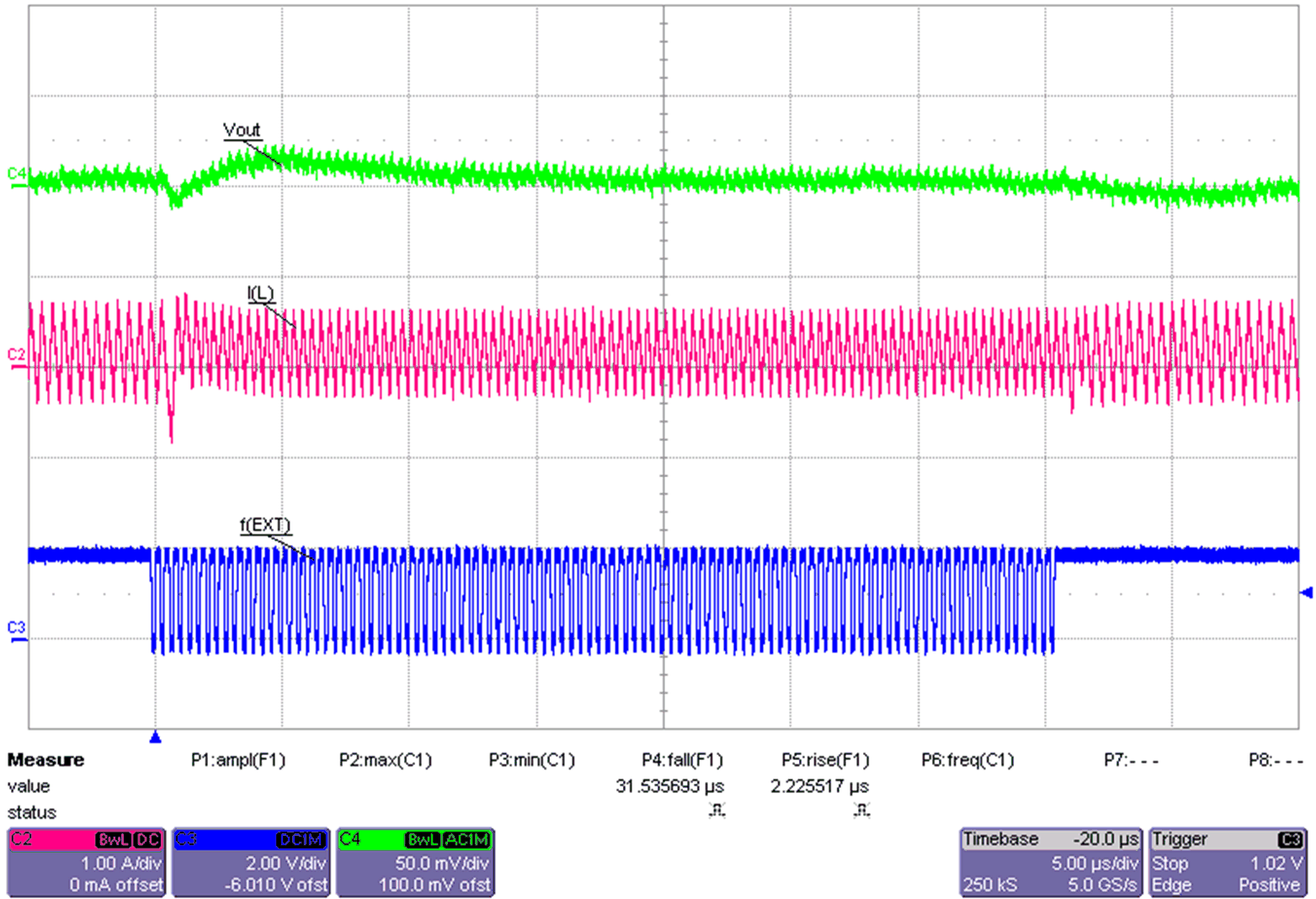
The TPS62850x-Q1 can be externally synchronized by applying an external clock on the MODE/SYNC pin. There is no need for any additional circuitry as long as the input signal meets the requirements given in the electrical specifications. The clock can be applied / removed during operation, allowing you to switch from an externally defined fixed frequency to power-save mode or to internal fixed frequency operation.

The value of the RCF resistor must be chosen such that the internally defined frequency and the externally applied frequency are close to each other. This ensures a smooth transition from internal to external frequency and vice versa.
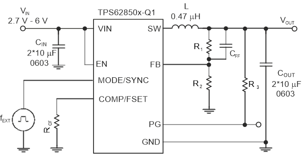
TPS628501-Q1 TPS628502-Q1 TPS628503-Q1 Schematic using External SynchronizationFigure 9-58 Schematic using External Synchronization
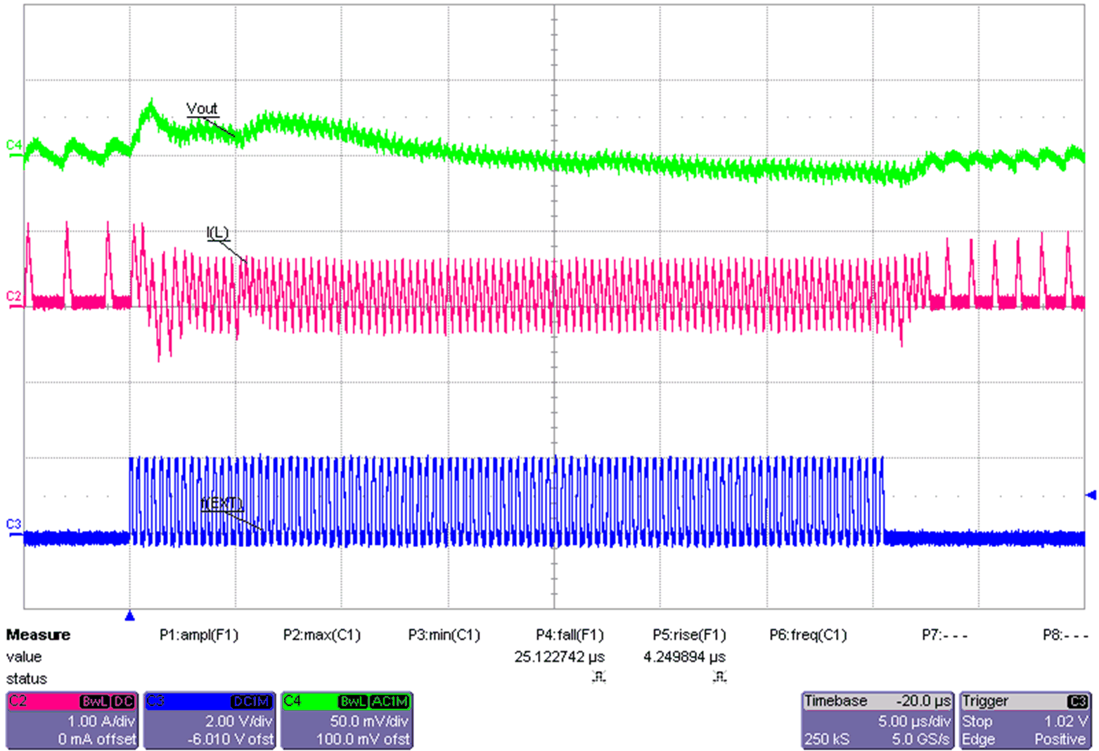
TPS628501-Q1 TPS628502-Q1 TPS628503-Q1 Switching from External Syncronization to Power-Save Mode (PFM)
VIN = 5 VRCF = 8.06 kΩIOUT = 0.1 A
VOUT = 1.8 VfEXT = 2.5 MHz
Figure 9-59 Switching from External Syncronization to Power-Save Mode (PFM)
TPS628501-Q1 TPS628502-Q1 TPS628503-Q1 Switching from External Synchronizaion to Internal Fixed Frequency
VIN = 5 VRCF = 8.06 kΩIOUT = 0.1 A
VOUT = 1.8 VfEXT = 2.5 MHz
Figure 9-60 Switching from External Synchronizaion to Internal Fixed Frequency