SLUSDM0K May   2020  – June 2024 TPS628501-Q1 , TPS628502-Q1 , TPS628503-Q1

PRODMIX  

  1.   1
  2. Features
  3. Applications
  4. Description
  5. Device Comparison Table
  6. Pin Configuration and Functions
  7. Specifications
    1. 6.1 Absolute Maximum Ratings
    2. 6.2 ESD Ratings
    3. 6.3 Recommended Operating Conditions
    4. 6.4 Thermal Information
    5. 6.5 Electrical Characteristics
    6. 6.6 Typical Characteristics
  8. Parameter Measurement Information
    1. 7.1 Schematic
  9. Detailed Description
    1. 8.1 Overview
    2. 8.2 Functional Block Diagram
    3. 8.3 Feature Description
      1. 8.3.1 Precise Enable (EN)
      2. 8.3.2 COMP/FSET
      3. 8.3.3 MODE / SYNC
      4. 8.3.4 Spread Spectrum Clocking (SSC)
      5. 8.3.5 Undervoltage Lockout (UVLO)
      6. 8.3.6 Power-Good Output (PG)
      7. 8.3.7 Thermal Shutdown
    4. 8.4 Device Functional Modes
      1. 8.4.1 Pulse Width Modulation (PWM) Operation
      2. 8.4.2 Power Save Mode Operation (PWM/PFM)
      3. 8.4.3 100% Duty-Cycle Operation
      4. 8.4.4 Current Limit and Short Circuit Protection
      5. 8.4.5 Foldback Current Limit and Short-Circuit Protection
      6. 8.4.6 Output Discharge
      7. 8.4.7 Input Overvoltage Protection
  10. Application and Implementation
    1. 9.1 Application Information
      1. 9.1.1 Programming the Output Voltage
      2. 9.1.2 External Component Selection
        1. 9.1.2.1 Inductor Selection
      3. 9.1.3 Capacitor Selection
        1. 9.1.3.1 Input Capacitor
        2. 9.1.3.2 Output Capacitor
    2. 9.2 Typical Application
      1. 9.2.1 Design Requirements
      2. 9.2.2 Detailed Design Procedure
      3. 9.2.3 Application Curves
    3. 9.3 System Examples
      1. 9.3.1 Fixed Output Voltage Versions
      2. 9.3.2 Synchronizing to an External Clock
    4. 9.4 Power Supply Recommendations
    5. 9.5 Layout
      1. 9.5.1 Layout Guidelines
      2. 9.5.2 Layout Example
  11. 10Device and Documentation Support
    1. 10.1 Device Support
      1. 10.1.1 Third-Party Products Disclaimer
    2. 10.2 Receiving Notification of Documentation Updates
    3. 10.3 Support Resources
    4. 10.4 Trademarks
    5. 10.5 Electrostatic Discharge Caution
    6. 10.6 Glossary
  12. 11Revision History
  13. 12Mechanical, Packaging, and Orderable Information

Package Options

Mechanical Data (Package|Pins)
Thermal pad, mechanical data (Package|Pins)
Orderable Information

Schematic

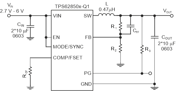
TPS628501-Q1 TPS628502-Q1 TPS628503-Q1 Measurement Setup (TPS62850x-Q1)Figure 7-1 Measurement Setup (TPS62850x-Q1)
Table 7-1 List of Components
REFERENCEDESCRIPTIONMANUFACTURER (1)
ICTPS628502QDRLRQ1Texas Instruments
L0.47-µH inductor DFE252012PDMurata
CIN2 × 10 µF / 6.3 V GCM188D70J106MMurata
COUT2 × 10 µF / 6.3 V GCM188D70J106M for Vout ≥ 1 VMurata
COUT3 × 10 µF / 6.3 V GCM188D70J106M for Vout < 1 VMurata
RCF8,06 kΩAny
CFF10 pFAny
R1Depending on VOUTAny
R2Depending on VOUTAny
R3100 kΩAny