SLUSEC8B March 2021 – April 2024 TPS628501 , TPS628502 , TPS628503
PRODUCTION DATA
- 1
- 1 Features
- 2 Applications
- 3 Description
- 4 Device Comparison Table
- 5 Pin Configuration and Functions
- 6 Specifications
- 7 Parameter Measurement Information
-
8 Detailed Description
- 8.1 Overview
- 8.2 Functional Block Diagram
- 8.3 Feature Description
- 8.4
Device Functional Modes
- 8.4.1 Pulse Width Modulation (PWM) Operation
- 8.4.2 Power Save Mode Operation (PWM/PFM)
- 8.4.3 100% Duty-Cycle Operation
- 8.4.4 Current Limit and Short Circuit Protection
- 8.4.5 Foldback Current Limit and Short Circuit Protection
- 8.4.6 Output Discharge
- 8.4.7 Soft Start
- 8.4.8 Input Overvoltage Protection
- 9 Application and Implementation
- 10Device and Documentation Support
- 11Revision History
- 12Mechanical, Packaging, and Orderable Information
Package Options
Mechanical Data (Package|Pins)
- DRL|8
Thermal pad, mechanical data (Package|Pins)
Orderable Information
3 Description
The TPS62850x is a family of pin-to-pin 1A, 2A (continuous), and 3A (peak) high efficiency, easy-to-use synchronous step-down DC/DC converters. The devices are based on a peak current mode control topology. Low resistive switches allow up to 2A continuous output current and 3A peak current. The switching frequency is externally adjustable from 1.8MHz to 4MHz and can also be synchronized to an external clock in the same frequency range. In PWM and PFM mode, the TPS62850x automatically enters power save mode at light loads to maintain high efficiency across the whole load range. The TPS62850x provides a 1% output voltage accuracy in PWM mode, which helps design a power supply with high output voltage accuracy, fulfilling tight supply voltage requirements of digital processors and FPGA.
The TPS62850x is available in an 8-pin 1.60mm × 2.10mm SOT583 package.
| PART NUMBER | PACKAGE(1) | PACKAGE SIZE(2) |
|---|---|---|
| TPS62850x | DRL (SOT583, 8) | 1.60mm × 2.10mm |
| PART NUMBER(1) | OUTPUT CURRENT | OUTPUT VOLTAGE |
|---|---|---|
| TPS628501DRLR | 1A | Adjustable |
| Fixed 1.8V | ||
| TPS628502DRLR | 2A | Adjustable |
| TPS628502ADRLR | Fixed 1.2V | |
| TPS628502MDRLR | Fixed 1.8V | |
| TPS628503DRLR | 3A | Adjustable |
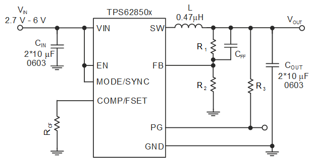
 Simplified Schematic
 Efficiency versus IOUT,
VOUT = 3.3 V