SLUSFG2A September   2024  – November 2024 TPS6286A06 , TPS6286B10

PRODMIX  

  1.   1
  2. Features
  3. Applications
  4. Description
  5. Device Options
  6. Pin Configuration and Functions
  7. Specifications
    1. 6.1 Absolute Maximum Rating
    2. 6.2 ESD Ratings
    3. 6.3 Recommended Operating Conditions
    4. 6.4 Thermal Information
    5. 6.5 Electrical Characteristics
    6. 6.6 I2C Interface Timing Requirements
    7. 6.7 Typical Characteristics
  8. Detailed Description
    1. 7.1 Overview
    2. 7.2 Functional Block Diagram
    3. 7.3 Feature Description
      1. 7.3.1 Power Save Mode (PFM)
      2. 7.3.2 Forced PWM Mode
      3. 7.3.3 Low Dropout Operation (100% Duty Cycle)
      4. 7.3.4 Soft Start
      5. 7.3.5 Switch Current Limit and HICCUP Short-Circuit Protection
      6. 7.3.6 Undervoltage Lockout
      7. 7.3.7 Thermal Warning and Shutdown
    4. 7.4 Device Functional Modes
      1. 7.4.1 Enable and Disable (EN)
      2. 7.4.2 Output Discharge
      3. 7.4.3 Power Good (PG)
      4. 7.4.4 Voltage Setting and Mode Selection (VSET/MODE), TPS6286Axx Devices
    5. 7.5 Programming
      1. 7.5.1 Serial Interface Description
      2. 7.5.2 Standard-, Fast-, and Fast-Mode Plus Protocol
      3. 7.5.3 HS Mode Protocol
      4. 7.5.4 I2C Update Sequence
      5. 7.5.5 I2C Register Reset
  9. Register Map
    1. 8.1 Target Address Byte
    2. 8.2 Register Address Byte
    3. 8.3 VOUT Register
    4. 8.4 CONTROL Register
    5. 8.5 STATUS Register
  10. Application and Implementation
    1. 9.1 Application Information
    2. 9.2 Typical Application
      1. 9.2.1 Design Requirements
      2. 9.2.2 Detailed Design Procedure
        1. 9.2.2.1 Custom Design With WEBENCH® Tools
        2. 9.2.2.2 Setting the Output Voltage
        3. 9.2.2.3 Output Filter Design
        4. 9.2.2.4 Inductor Selection
        5. 9.2.2.5 Capacitor Selection
      3. 9.2.3 Application Curves
    3. 9.3 Power Supply Recommendations
    4. 9.4 Layout
      1. 9.4.1 Layout Guidelines
      2. 9.4.2 Layout Example
        1. 9.4.2.1 Thermal Considerations
  11. 10Device and Documentation Support
    1. 10.1 Device Support
      1. 10.1.1 Third-Party Products Disclaimer
      2. 10.1.2 Development Support
        1. 10.1.2.1 Custom Design With WEBENCH® Tools
    2. 10.2 Documentation Support
      1. 10.2.1 Related Documentation
    3. 10.3 Receiving Notification of Documentation Updates
    4. 10.4 Support Resources
    5. 10.5 Trademarks
    6. 10.6 Electrostatic Discharge Caution
    7. 10.7 Glossary
  12. 11Revision History
  13. 12Mechanical, Packaging, and Orderable Information

Package Options

Mechanical Data (Package|Pins)
  • VBM|13
Thermal pad, mechanical data (Package|Pins)
Orderable Information

Application Curves

VIN = 5.0V, VOUT = 1.2V, TA = 25°C, BOM = Table 9-2, unless otherwise noted. Solid lines show the FPWM mode and dashed lines show PFM.

TPS6286A06 TPS6286B10 Efficiency vs Output Current
VIN= 5VTA = 25°CPFM and FPWM
Figure 9-4 Efficiency vs Output Current
TPS6286A06 TPS6286B10 Efficiency vs Output Current
VIN = 5VTA = 85°CPFM and FPWM
Figure 9-6 Efficiency vs Output Current
TPS6286A06 TPS6286B10 Efficiency vs Output Current
VIN = 5VTA = 85°CFPWM
Figure 9-8 Efficiency vs Output Current
TPS6286A06 TPS6286B10 Load Regulation
VIN = 5VTA = 25°CPFM
Figure 9-10 Load Regulation
TPS6286A06 TPS6286B10 Load Regulation
VIN = 5VTA = 25°CFPWM
Figure 9-12 Load Regulation
TPS6286A06 TPS6286B10 Switching Frequency
VIN = 3.3VTA = 25°CPFM
Figure 9-14 Switching Frequency
TPS6286A06 TPS6286B10 Safe Operating Area
VIN = 5.0VRθJA = 43.2°C/W

TJMAX= 125°C

Figure 9-16 Safe Operating Area
TPS6286A06 TPS6286B10 Line Regulation
VIN = 2.4V to 5.5V to 2.4V in 1V/usVOUT = 1.2VLoad = 10mA
Figure 9-18 Line Regulation
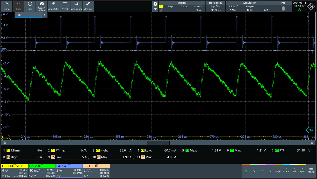
TPS6286A06 TPS6286B10 PFM Operation
VIN = 5.0VBOM = 2 × 22uF
VOUT = 1.2VPFM, No Load
Figure 9-20 PFM Operation
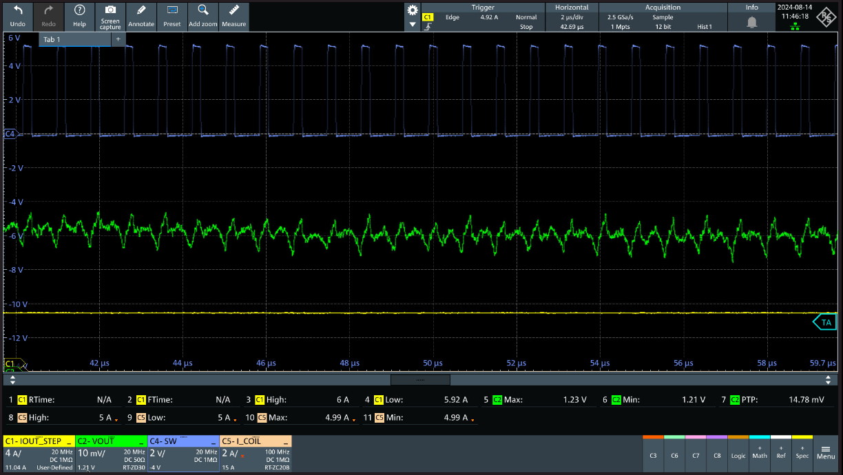
TPS6286A06 TPS6286B10 FPWM Operation
VIN = 5.0VBOM = 2 × 22uF
VOUT = 1.2VFPWM, IOUT = 6A
Figure 9-22 FPWM Operation
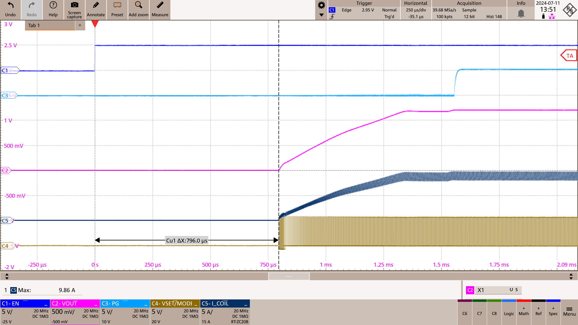
TPS6286A06 TPS6286B10 Start-Up into Full Load
TPS6286B10VOUT = 1.2VLoad = 10A
Figure 9-24 Start-Up into Full Load
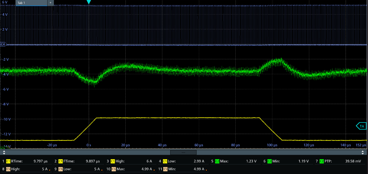
TPS6286A06 TPS6286B10 Load Transient - PFM Operation
VIN = 5.0VBOM = 2 × 22uF
VOUT = 1.2VIOUT = 10mA to 6A, 1A/μs
Figure 9-26 Load Transient - PFM Operation
TPS6286A06 TPS6286B10 Load Transient - FPWM Operation
VIN = 5.0VBOM = 2 × 22uF
VOUT = 1.2VIOUT = 3A to 6A, 1A/μs
Figure 9-28 Load Transient - FPWM Operation
TPS6286A06 TPS6286B10 Load Transient - FPWM Operation
VIN = 5.0VBOM = 4 × 22uF
VOUT = 1.2VIOUT = 10mA to 10A, 1A/μs
Figure 9-30 Load Transient - FPWM Operation
TPS6286A06 TPS6286B10 Load Transient - PFM Operation
VIN = 5.0VBOM = 4 × 22uF
VOUT = 0.9VIOUT = 10mA to 10A, 1A/μs
Figure 9-32 Load Transient - PFM Operation
TPS6286A06 TPS6286B10 Load Transient - PFM Operation
VIN = 5.0VBOM = 4 × 22uF
VOUT = 0.9VIOUT = 4A to 10A, 1A/μs
Figure 9-34 Load Transient - PFM Operation
TPS6286A06 TPS6286B10 Efficiency vs Output Current
VIN = 3.3VTA = 25°CPFM and FPWM
Figure 9-5 Efficiency vs Output Current
TPS6286A06 TPS6286B10 Efficiency vsOutput Current
VIN = 3.3VTA = 85°CPFM and FPWM
Figure 9-7 Efficiency vsOutput Current
TPS6286A06 TPS6286B10 Efficiency vs Output Current
VIN = 3.3VTA = 85°CFPWM
Figure 9-9 Efficiency vs Output Current
TPS6286A06 TPS6286B10 Load Regulation
VIN = 3.3VTA = 25°C

PFM

Figure 9-11 Load Regulation
TPS6286A06 TPS6286B10 Load Regulation
VIN = 3.3VTA = 25°CFPWM
Figure 9-13 Load Regulation
TPS6286A06 TPS6286B10 Switching Frequency
VIN = 5.0VTA = 25°CPFM
Figure 9-15 Switching Frequency
TPS6286A06 TPS6286B10 Safe Operating Area
VIN = 3.3VRθJA = 43.2°C/WTJMAX = 125°C
Figure 9-17 Safe Operating Area
TPS6286A06 TPS6286B10 Line Regulation
VIN = 2.4V to 5.5V to 2.4V in 1V/usVOUT = 1.2VLoad = 10A
Figure 9-19 Line Regulation
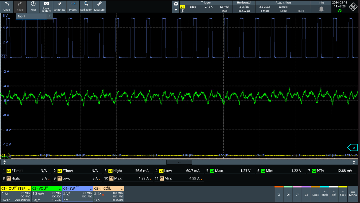
TPS6286A06 TPS6286B10 FPWM Operation
VIN = 5.0VBOM = 2 × 22uF
VOUT = 1.2VFPWM, No Load
Figure 9-21 FPWM Operation
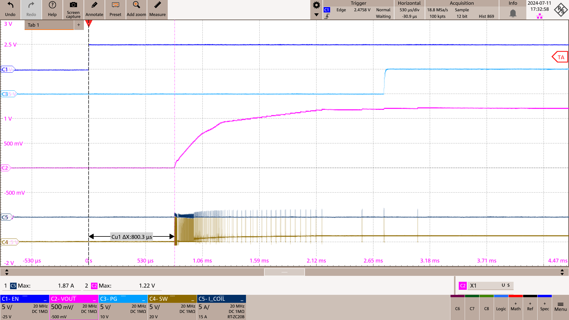
TPS6286A06 TPS6286B10 Start-Up With No Load
TPS6286A06VOUT = 1.2VNo Load
Figure 9-23 Start-Up With No Load
TPS6286A06 TPS6286B10 External Soft Start and Shutdown into No Load
TPS6286B10VOUT = 1.6VCSS = 100nF
Figure 9-25 External Soft Start and Shutdown into No Load
TPS6286A06 TPS6286B10 Load Transient - FPWM Operation
VIN = 5.0VBOM = 2 × 22uF
VOUT = 1.2VIOUT = 10mA to 6A, 1A/μs
Figure 9-27 Load Transient - FPWM Operation
TPS6286A06 TPS6286B10 Load Transient - PFM Operation
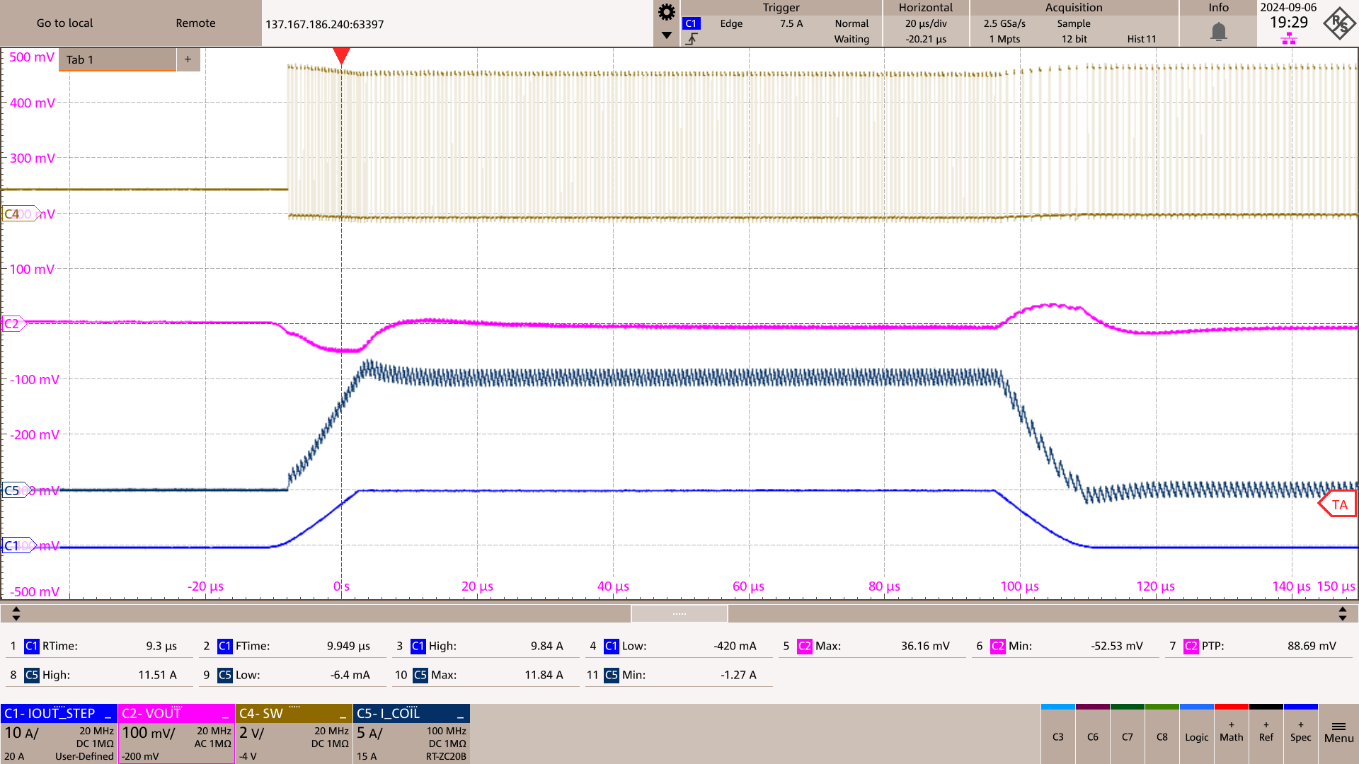
VIN = 5.0VBOM = 4 × 22uF
VOUT = 1.2VIOUT = 10mA to 10A, 1A/μs
Figure 9-29 Load Transient - PFM Operation
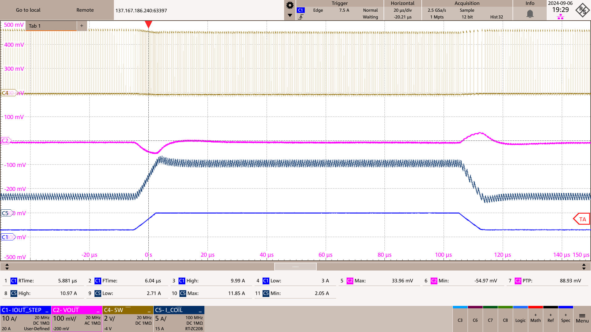
TPS6286A06 TPS6286B10 Load Transient - PFM Operation
VIN = 5.0VBOM = 4 × 22uF
VOUT = 1.2VIOUT = 4A to 10A, 1A/μs
Figure 9-31 Load Transient - PFM Operation
TPS6286A06 TPS6286B10 Load Transient - FPWM Operation
VIN = 5.0VBOM = 4 × 22uF
VOUT = 0.9VIOUT = 10mA to 10A, 1A/μs
Figure 9-33 Load Transient - FPWM Operation
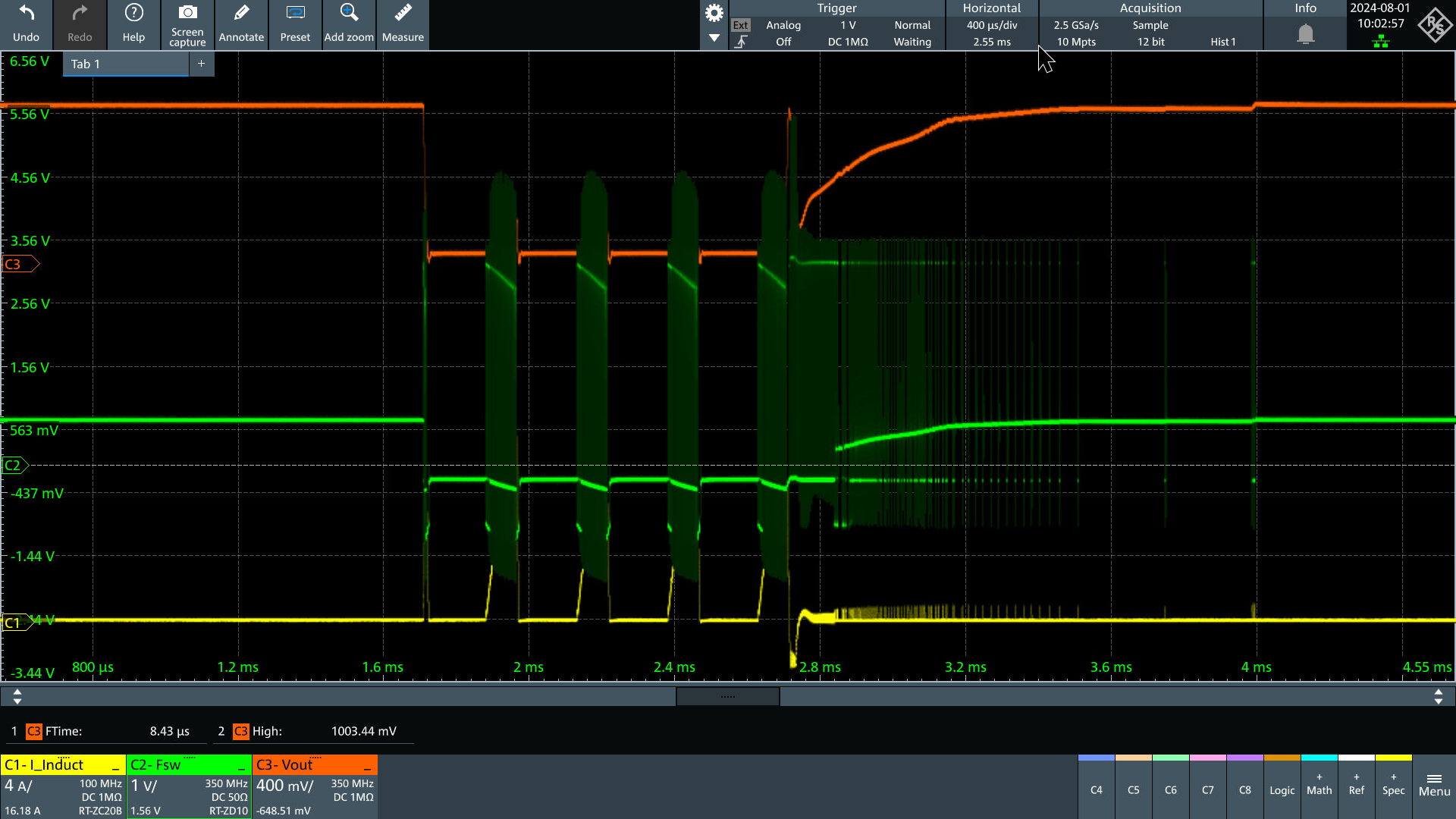
TPS6286A06 TPS6286B10 HICCUP Short-Circuit ProtectionFigure 9-35 HICCUP Short-Circuit Protection