SLVSGG8C November   2023  – October 2024 TPS6287B10 , TPS6287B15 , TPS6287B20 , TPS6287B25 , TPS6287B30

PRODUCTION DATA  

  1.   1
  2. Features
  3. Applications
  4. Description
  5. Device Options
  6. Pin Configuration and Functions
  7. Specifications
    1. 6.1 Absolute Maximum Ratings
    2. 6.2 ESD Ratings
    3. 6.3 Recommended Operating Conditions
    4. 6.4 Thermal Information
    5. 6.5 Electrical Characteristics
    6. 6.6 I2C Interface Timing Characteristics
    7. 6.7 Typical Characteristics
  8. Parameter Measurement Information
  9. Detailed Description
    1. 8.1 Overview
    2. 8.2 Functional Block Diagram
    3. 8.3 Feature Description
      1. 8.3.1  Fixed-Frequency DCS-Control Topology
      2. 8.3.2  Forced-PWM and Power-Save Modes
      3. 8.3.3  Transient Non-Synchronous Mode (optional)
      4. 8.3.4  Precise Enable
      5. 8.3.5  Start-Up
      6. 8.3.6  Switching Frequency Selection, Only Applies to TPS6287BxxJE2
      7. 8.3.7  Output Voltage Setting
        1. 8.3.7.1 Output Voltage Range
        2. 8.3.7.2 Output Voltage Setpoint
        3. 8.3.7.3 Non-Default Output Voltage Setpoint
        4. 8.3.7.4 Dynamic Voltage Scaling
        5. 8.3.7.5 Droop Compensation
      8. 8.3.8  Compensation (COMP)
      9. 8.3.9  Mode Selection / Clock Synchronization (MODE/SYNC)
      10. 8.3.10 Spread Spectrum Clocking (SSC)
      11. 8.3.11 Output Discharge
      12. 8.3.12 Undervoltage Lockout (UVLO)
      13. 8.3.13 Overvoltage Lockout (OVLO)
      14. 8.3.14 Overcurrent Protection
        1. 8.3.14.1 Cycle-by-Cycle Current Limiting
        2. 8.3.14.2 Hiccup Mode
        3. 8.3.14.3 Current-Limit Mode
      15. 8.3.15 Power Good (PG)
        1. 8.3.15.1 Standalone, Primary Device Behavior
        2. 8.3.15.2 Secondary Device Behavior
      16. 8.3.16 Remote Sense
      17. 8.3.17 Thermal Warning and Shutdown
      18. 8.3.18 Stacked Operation
    4. 8.4 Device Functional Modes
      1. 8.4.1 Power-On Reset
      2. 8.4.2 Undervoltage Lockout
      3. 8.4.3 Standby
      4. 8.4.4 On
    5. 8.5 Programming
      1. 8.5.1 Serial Interface Description
      2. 8.5.2 Standard-, Fast-, Fast-Mode Plus Protocol
      3. 8.5.3 HS-Mode Protocol
      4. 8.5.4 I2C Update Sequence
      5. 8.5.5 I2C Register Reset
      6. 8.5.6 Dynamic Voltage Scaling (DVS)
  10. Device Registers
  11. 10Application and Implementation
    1. 10.1 Application Information
    2. 10.2 Typical Application
      1. 10.2.1 Design Requirements
      2. 10.2.2 Detailed Design Procedure
        1. 10.2.2.1 Inductor Selection
        2. 10.2.2.2 Selecting the Input Capacitors
        3. 10.2.2.3 Selecting the Compensation Resistor
        4. 10.2.2.4 Selecting the Output Capacitors
        5. 10.2.2.5 Selecting the Compensation Capacitor CC
        6. 10.2.2.6 Selecting the Compensation Capacitor CC2
      3. 10.2.3 Application Curves
    3. 10.3 Typical Application - TPS6287BxV Devices
      1. 10.3.1 Design Requirements for TPS6287BxV
    4. 10.4 Typical Application Using Two TPS6287B25 in a Stacked Configuration
      1. 10.4.1 Design Requirements For Two Stacked Devices
      2. 10.4.2 Detailed Design Procedure
        1. 10.4.2.1 Selecting the Compensation Resistor
        2. 10.4.2.2 Selecting the Output Capacitors
        3. 10.4.2.3 Selecting the Compensation Capacitor CC
      3. 10.4.3 Application Curves for Two Stacked Devices
    5. 10.5 Typical Application Using Three TPS6287B25 in a Stacked Configuration
      1. 10.5.1 Application Curves
    6. 10.6 Power Supply Recommendations
    7. 10.7 Layout
      1. 10.7.1 Layout Guidelines
      2. 10.7.2 Layout Example
  12. 11Device and Documentation Support
    1. 11.1 Documentation Support
      1. 11.1.1 Related Documentation
    2. 11.2 Receiving Notification of Documentation Updates
    3. 11.3 Support Resources
    4. 11.4 Trademarks
    5. 11.5 Electrostatic Discharge Caution
    6. 11.6 Glossary
  13. 12Revision History
  14. 13Mechanical, Packaging, and Orderable Information

Package Options

Mechanical Data (Package|Pins)
Thermal pad, mechanical data (Package|Pins)
Orderable Information

Application Curves

TPS6287B10 TPS6287B15 TPS6287B20 TPS6287B25 TPS6287B30 Efficiency Versus Output Current
VIN = 5.0V

FPWM

TA = 25°C
Figure 10-2 Efficiency Versus Output Current
TPS6287B10 TPS6287B15 TPS6287B20 TPS6287B25 TPS6287B30 Efficiency Versus Output Current
VIN = 3.3VFPWMTA = 25°C
Figure 10-4 Efficiency Versus Output Current
TPS6287B10 TPS6287B15 TPS6287B20 TPS6287B25 TPS6287B30 Safe Operating Area
VIN = 5.0VNat. convectionTJMAX = 125°C
Figure 10-6 Safe Operating Area
TPS6287B10 TPS6287B15 TPS6287B20 TPS6287B25 TPS6287B30 Output Voltage Versus Output Current
VIN = 5.0V FPWM; TPS6287B25 droop disabled VOUT = 0.4V
Figure 10-8 Output Voltage Versus Output Current
TPS6287B10 TPS6287B15 TPS6287B20 TPS6287B25 TPS6287B30 Output Voltage Versus Output Current
VIN = 5.0V FPWM; TPS6287B25 droop disabled VOUT = 0.8V
Figure 10-10 Output Voltage Versus Output Current
TPS6287B10 TPS6287B15 TPS6287B20 TPS6287B25 TPS6287B30 Output Voltage Versus Output Current
VIN = 5.0V FPWM; TPS6287B25 droop disabled VOUT = 1.675V
Figure 10-12 Output Voltage Versus Output Current
TPS6287B10 TPS6287B15 TPS6287B20 TPS6287B25 TPS6287B30 Output Voltage Versus Output Current
VIN = 3.3V FPWM; TPS6287B25 droop disabled VOUT = 0.4V
Figure 10-14 Output Voltage Versus Output Current
TPS6287B10 TPS6287B15 TPS6287B20 TPS6287B25 TPS6287B30 Output Voltage Versus Output Current
VIN = 3.3V FPWM; TPS6287B25 droop disabled VOUT = 0.8V
Figure 10-16 Output Voltage Versus Output Current
TPS6287B10 TPS6287B15 TPS6287B20 TPS6287B25 TPS6287B30 Output Voltage Versus Output Current
VIN = 3.3V FPWM; TPS6287B25 droop disabled VOUT = 1.675V
Figure 10-18 Output Voltage Versus Output Current
TPS6287B10 TPS6287B15 TPS6287B20 TPS6287B25 TPS6287B30 Start-Up Timing
VOUT = 0.75VPWMTA = 25°C
VIN = 5VRLOAD = 66mΩ
Figure 10-20 Start-Up Timing
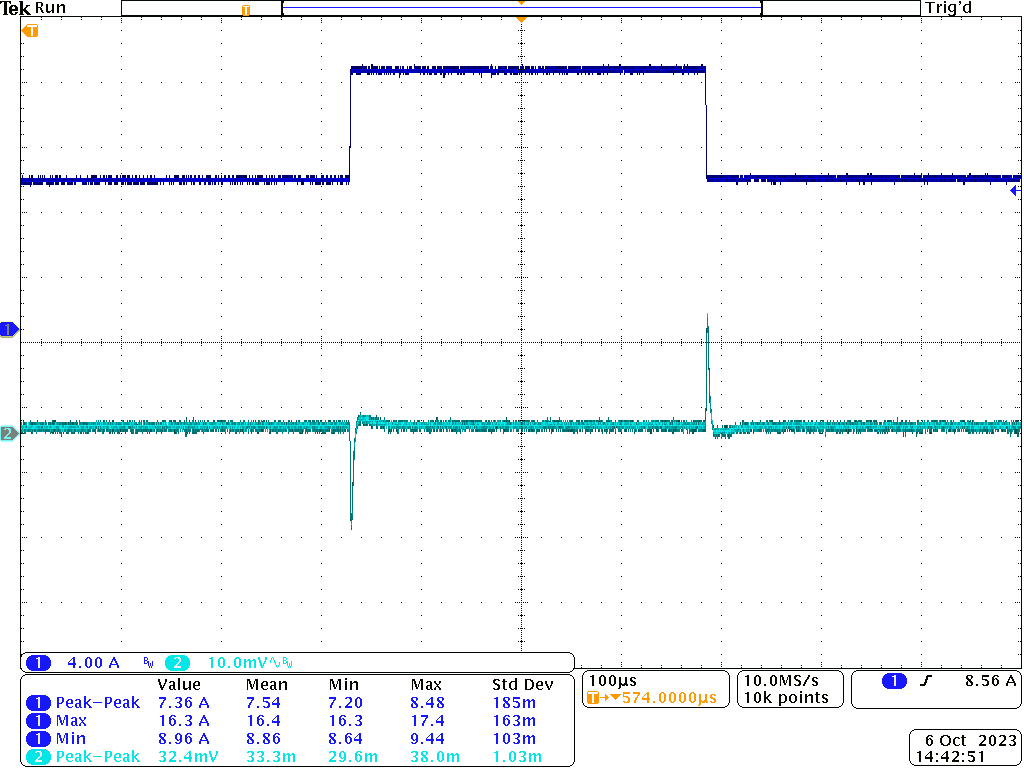
TPS6287B10 TPS6287B15 TPS6287B20 TPS6287B25 TPS6287B30 Load Transient Response
VOUT = 0.75V

PWM, TPS6287B25 droop disabled

TA = 25°C

VIN = 3.3V

Iout = 8.75A to 16.25A to 8.75A

Figure 10-22 Load Transient Response
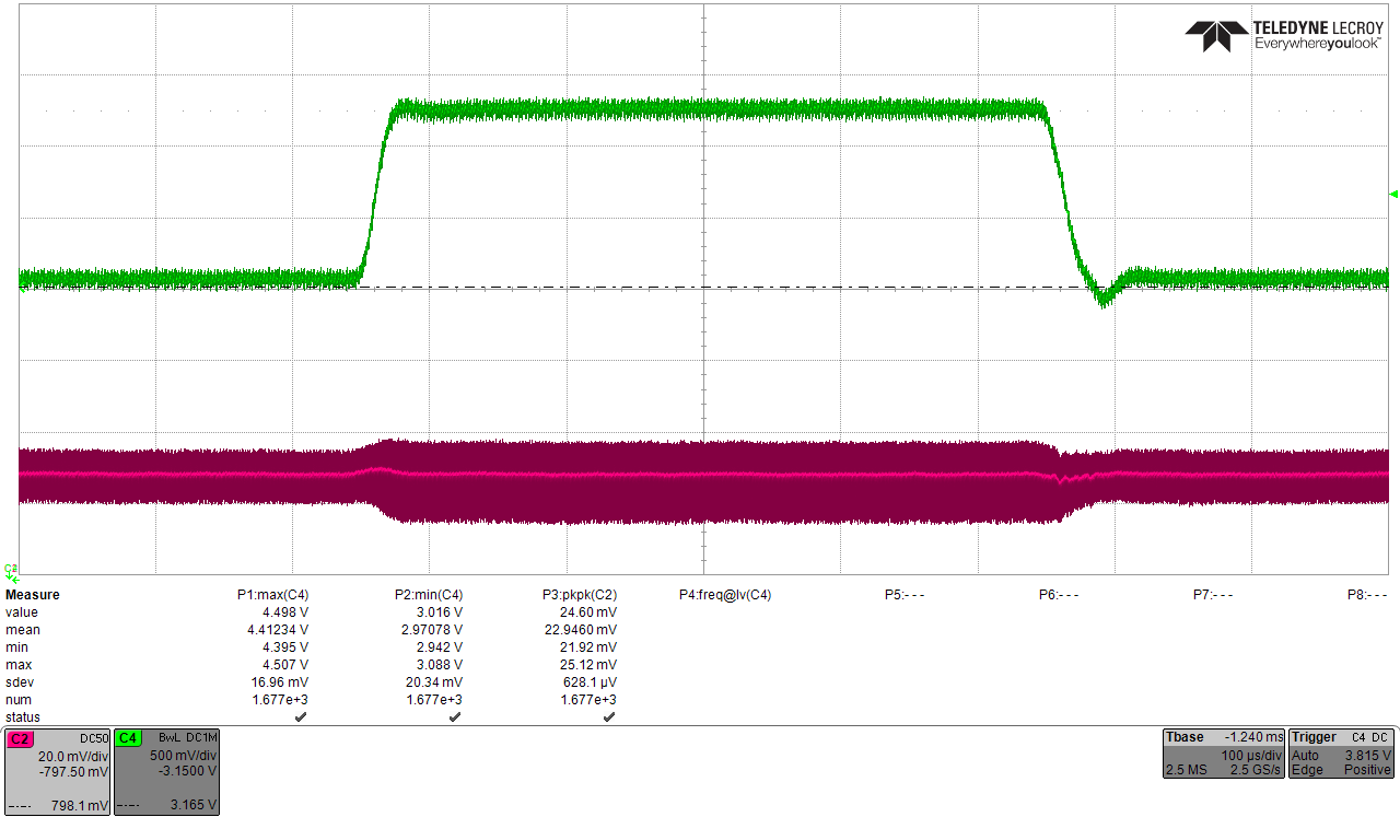
TPS6287B10 TPS6287B15 TPS6287B20 TPS6287B25 TPS6287B30 Line Transient Response
VOUT = 0.75V

FPWM

TA = 25°C

VIN = 3.0V to 4.5V to 3.0V

IOUT = 16.25A

Figure 10-24 Line Transient Response
TPS6287B10 TPS6287B15 TPS6287B20 TPS6287B25 TPS6287B30 Efficiency Versus Output Current
VIN = 5.0VFPWMTA = 85°C
Figure 10-3 Efficiency Versus Output Current
TPS6287B10 TPS6287B15 TPS6287B20 TPS6287B25 TPS6287B30 Efficiency Versus Output Current
VIN = 3.3VFPWMTA = 85°C
Figure 10-5 Efficiency Versus Output Current
TPS6287B10 TPS6287B15 TPS6287B20 TPS6287B25 TPS6287B30 Safe Operating Area
VIN = 3.3VNat. convectionTJMAX = 125°C
Figure 10-7 Safe Operating Area
TPS6287B10 TPS6287B15 TPS6287B20 TPS6287B25 TPS6287B30 Output Voltage Versus Output Current
VIN = 5.0V FPWM; TPS6287B25 droop enabled VOUT = 0.4V
Figure 10-9 Output Voltage Versus Output Current
TPS6287B10 TPS6287B15 TPS6287B20 TPS6287B25 TPS6287B30 Output Voltage Versus Output Current
VIN = 5.0V FPWM; TPS6287B25 droop enabled VOUT = 0.8V
Figure 10-11 Output Voltage Versus Output Current
TPS6287B10 TPS6287B15 TPS6287B20 TPS6287B25 TPS6287B30 Output Voltage Versus Output Current
VIN = 5.0V FPWM; TPS6287B25 droop enabled VOUT = 1.675V
Figure 10-13 Output Voltage Versus Output Current
TPS6287B10 TPS6287B15 TPS6287B20 TPS6287B25 TPS6287B30 Output Voltage Versus Output Current
VIN = 3.3V FPWM; TPS6287B25 droop enabled VOUT = 0.4V
Figure 10-15 Output Voltage Versus Output Current
TPS6287B10 TPS6287B15 TPS6287B20 TPS6287B25 TPS6287B30 Output Voltage Versus Output Current
VIN = 3.3V FPWM; TPS6287B25 droop enabled VOUT = 0.8V
Figure 10-17 Output Voltage Versus Output Current
TPS6287B10 TPS6287B15 TPS6287B20 TPS6287B25 TPS6287B30 Output Voltage Versus Output Current
VIN = 3.3V FPWM; TPS6287B25 droop enabled VOUT = 1.675V
Figure 10-19 Output Voltage Versus Output Current
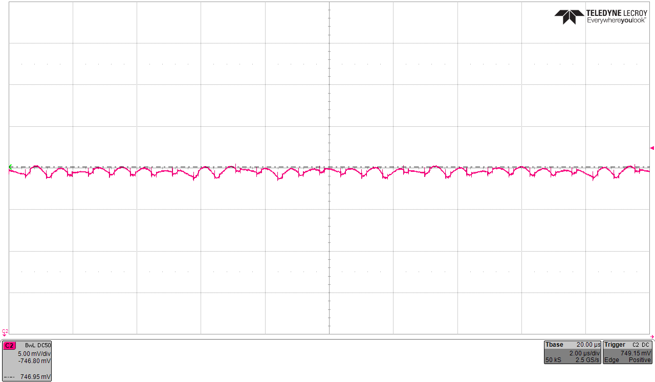
TPS6287B10 TPS6287B15 TPS6287B20 TPS6287B25 TPS6287B30 Output Voltage Ripple
VOUT = 0.75V

PWM

TA = 25°C

VIN = 3.3V

Iout = 11.3A

Figure 10-21 Output Voltage Ripple
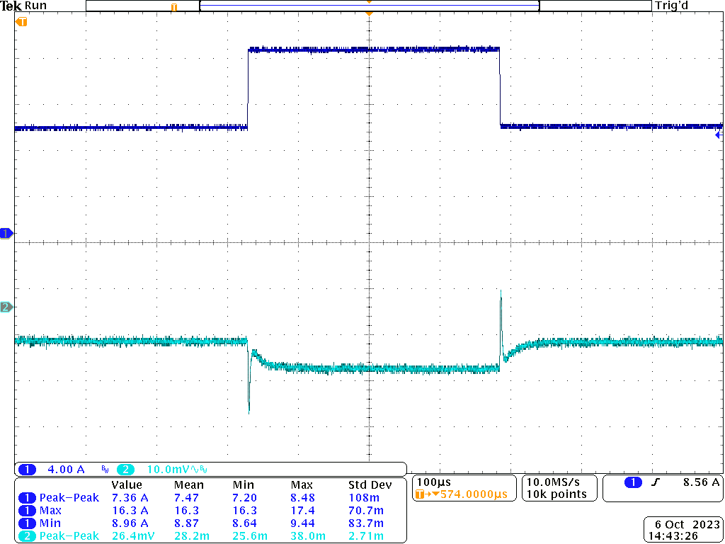
TPS6287B10 TPS6287B15 TPS6287B20 TPS6287B25 TPS6287B30 Load Transient Response
VOUT = 0.75V

PWM, TPS6287B25 droop enabled

TA = 25°C

VIN = 3.3V

Iout = 8.75A to 16.25A to 8.75A

Figure 10-23 Load Transient Response